SLVUA33A March   2014  – July 2021 TPS563900


  1.   Trademarks
  2. 1Introduction
    1. 1.1 Background
    2. 1.2 Performance Specification Summary
    3. 1.3 Modifications
      1. 1.3.1 Output Voltage Setpoint
      2. 1.3.2 Slow-Start Time
      3. 1.3.3 Adjustable UVLO
  3. 2Test Setup and Results
    1. 2.1 Input/Output Connections
    2. 2.2 Efficiency
    3. 2.3 Output Voltage Load Regulation
    4. 2.4 Output Voltage Line Regulation
    5. 2.5 Load Transients
    6. 2.6 Loop Characteristics
    7. 2.7 Output Voltage Ripple
    8. 2.8 Powering Up
    9. 2.9 Shutting Down
  4. 3Board Layout
    1. 3.1 Layout
  5. 4Schematic and Bill of Materials
    1. 4.1 Schematic
    2. 4.2 Bill of Materials
    3. 4.3 Reference
  6. 5Revision History

Shutting Down

Figure 2-25 shows the shut down waveforms for the TPS563900EVM-574 relative to EN1. EN2 is not shown, but the timing is the same relative to VIN and EN1. The input voltage for these plots is 12 V and the load is 1 Ω.
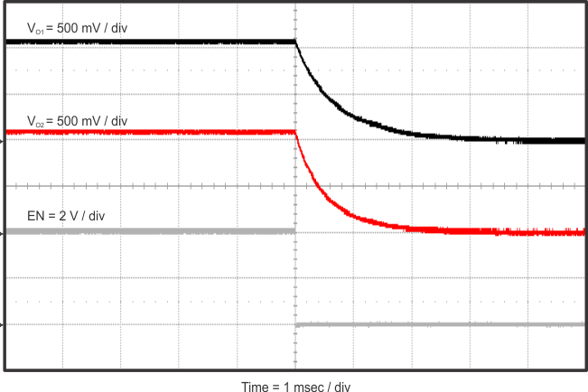
GUID-D9D2964C-DAAE-44F6-9215-B6A1870D6D7E-low.gifFigure 2-25 TPS563900EVM-574 Shut Down