SLVUAO9C March   2016  – June 2021 TPS56C215


  1.   Trademarks
  2. 1Introduction
    1. 1.1 Background
    2. 1.2 Performance Specification Summary
    3. 1.3 Modifications
      1. 1.3.1 Output Voltage Setpoint
      2. 1.3.2 Adjustable UVLO
  3. 2Test Setup and Results
    1. 2.1  Input/Output Connections
    2. 2.2  Efficiency
    3. 2.3  Output Voltage Load Regulation
    4. 2.4  Output Voltage Line Regulation
    5. 2.5  Load Transients
    6. 2.6  Loop Characteristics
    7. 2.7  Output Voltage Ripple
    8. 2.8  Input Voltage Ripple
    9. 2.9  Powering Up
    10. 2.10 Powering Down
  4. 3Board Layout
    1. 3.1 Layout
  5. 4Schematic and Bill of Materials
    1. 4.1 Schematic
    2. 4.2 Bill of Materials
  6. 5Revision History

Output Voltage Load Regulation

Figure 2-3 and Figure 2-4 show the load regulation for the TPS56C215EVM-762.
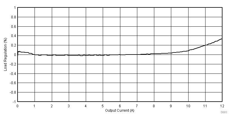
GUID-BD8A3C92-344E-4ED0-9F61-A435CFF9A89E-low.gifFigure 2-3 TPS56C215EVM-762 Load Regulation, VIN = 5 V
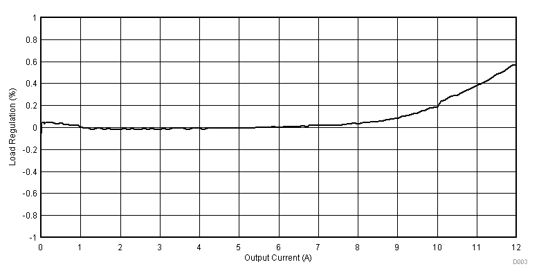
GUID-88484E8E-F214-42ED-84A1-2DC242813575-low.gifFigure 2-4 TPS56C215EVM-762 Load Regulation, VIN = 12 V

Measurements are given for an ambient temperature of 25°C.