SLVUAY5A October   2014  – July 2021 TPS563219A


  1.   Trademarks
  2. 1Introduction
  3. 2Performance Specification Summary
  4. 3Modifications
    1. 3.1 Output Voltage Setpoint
  5. 4Test Setup and Results
    1. 4.1  Input/Output Connections
    2. 4.2  Start-Up Procedure
    3. 4.3  Efficiency
    4. 4.4  Load Regulation
    5. 4.5  Line Regulation
    6. 4.6  Load Transient Response
    7. 4.7  Output Voltage Ripple
    8. 4.8  Input Voltage Ripple
    9. 4.9  Start-Up
    10. 4.10 Shut-Down
  6. 5Board Layout
    1. 5.1 Layout
  7. 6Schematic, Bill of Materials, and Reference
    1. 6.1 Schematic
    2. 6.2 Bill of Materials
    3. 6.3 Reference
  8. 7Revision History

Start-Up

The TPS563219AEVM-663 start-up waveform relative to VIN is shown in Figure 4-9. Load = 1 Ω resistive.
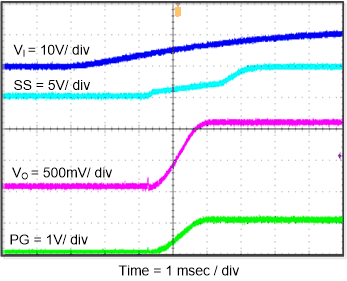
GUID-9B315656-0B8C-441C-AC7E-275E04276281-low.gifFigure 4-9 TPS563219AEVM-663 Start-Up Relative to VIN

The TPS563219AEVM-663 start-up waveform relative to enable (EN) is shown in Figure 4-10. Load = 1 Ω resistive.
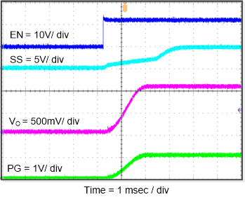
GUID-8862C836-C481-4F26-A9A4-2D43E0A1B35B-low.gifFigure 4-10 TPS563219AEVM-663 Start-Up Relative to EN