SLVUB76A July   2017  – October 2021 TPS54335A


  1.   Trademarks
  2. 1Introduction
    1. 1.1 Background
    2. 1.2 Performance Specification Summary
    3. 1.3 Modifications
      1. 1.3.1 Output Voltage Set Point
      2. 1.3.2 Adjustable UVLO
  3. 2Test Setup and Results
    1. 2.1  Input/Output Connections
    2. 2.2  Efficiency
    3. 2.3  Output Voltage Load Regulation
    4. 2.4  Output Voltage Line Regulation
    5. 2.5  Load Transients
    6. 2.6  Loop Characteristics
    7. 2.7  Output Voltage Ripple
    8. 2.8  Input Voltage Ripple
    9. 2.9  Powering Up
    10. 2.10 Powering Down
  4. 3Board Layout
    1. 3.1 Layout
  5. 4Schematic and Bill of Materials
    1. 4.1 Schematic
    2. 4.2 Bill of Materials
  6. 5Revision History

Input Voltage Ripple

Figure 2-10 shows the TPS54335AEVM-010 input voltage ripple. The output current is the rated full load of
3 A and VIN = 24 V. The ripple voltage is measured directly across the input capacitors.
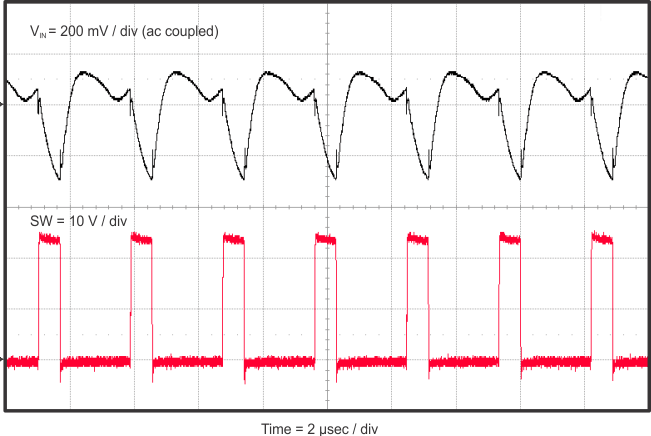
GUID-56A84249-B0E7-484B-8F3A-B258DFCB21CB-low.gifFigure 2-10 TPS54335AEVM-010 Input Ripple