SLVUBB4B November 2017 – February 2023
- Abstract
- Trademarks
- 1 Topologies Window
- 2 FET Losses Calculator
- 3 Load Step Calculator
- 4 Capacitor Current Sharing Calculator
- 5 AC/DC Bulk Capacitor Calculator
- 6 RCD-Snubber Calculator for Flyback Converters
- 7 RC-Snubber Calculator
- 8 Output Voltage Resistor Divider
- 9 Dynamic Analog Output Voltage Scaling
- 10Dynamic Digital Output Voltage Scaling
- 11Unit Converter
-
12Loop Calculator
- 12.1 Inputs
- 12.2
Transfer Functions
- 12.2.1 Output Impedance Transfer Function
- 12.2.2 Transfer Function VMC Buck Power Stage
- 12.2.3 Transfer Function CMC Buck Power Stage
- 12.2.4 Transfer Function CMC Boost Power Stage
- 12.2.5 Transfer Function CMC Inverting Buck-Boost Power Stage
- 12.2.6 Transfer Function CMC Forward Power Stage
- 12.2.7 Transfer Function CMC Flyback Power Stage
- 12.2.8 Transfer Function Closed Loop
- 12.2.9 Transfer Function Isolated Type II Compensation Network With a Zener Clamp
- 12.2.10 Transfer Function Isolated Type II Compensation Network Without a Zener Clamp
- 13Filter Designer
- 14Additional Information
- 15Revision History
1 Topologies Window
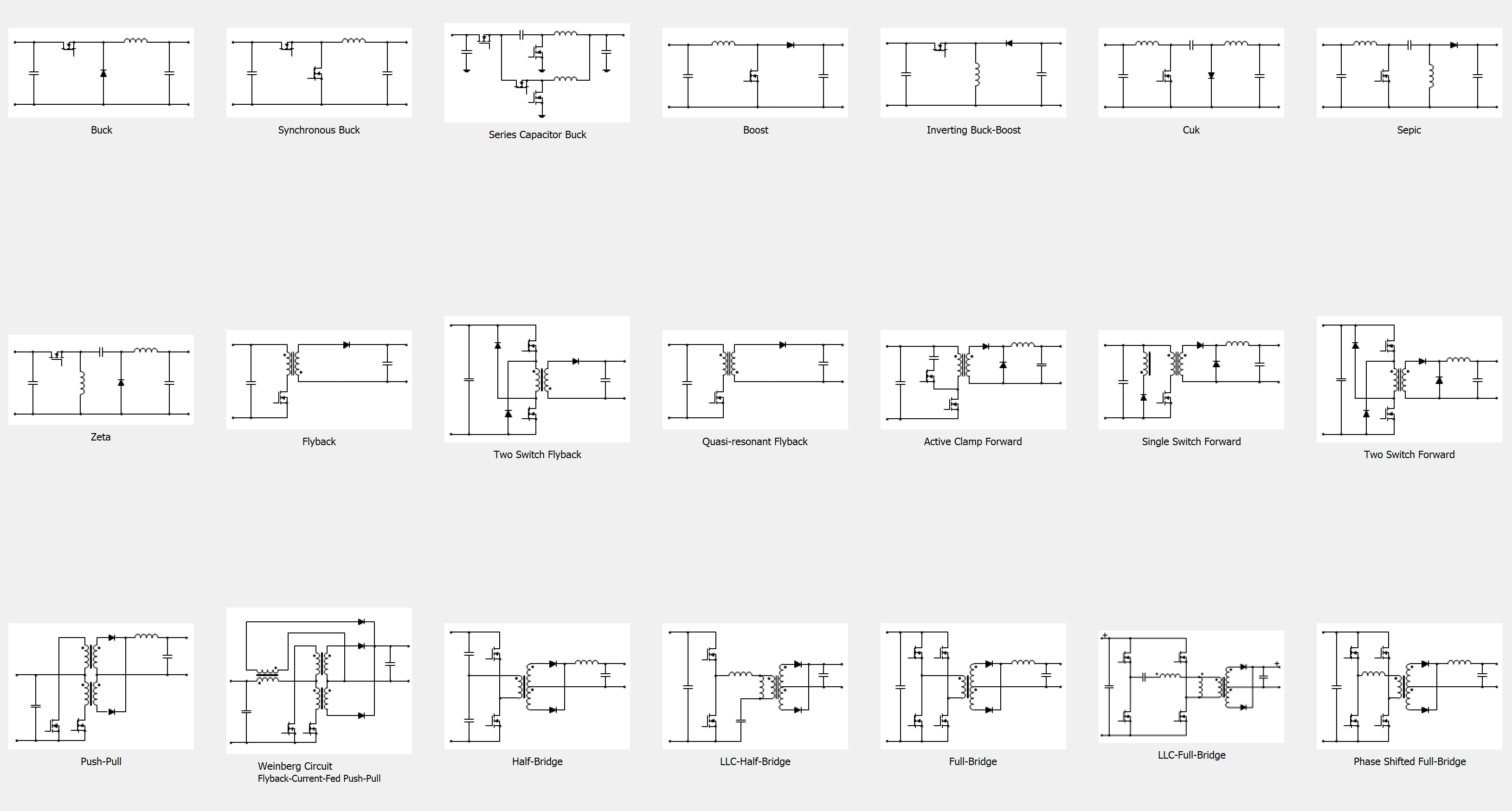
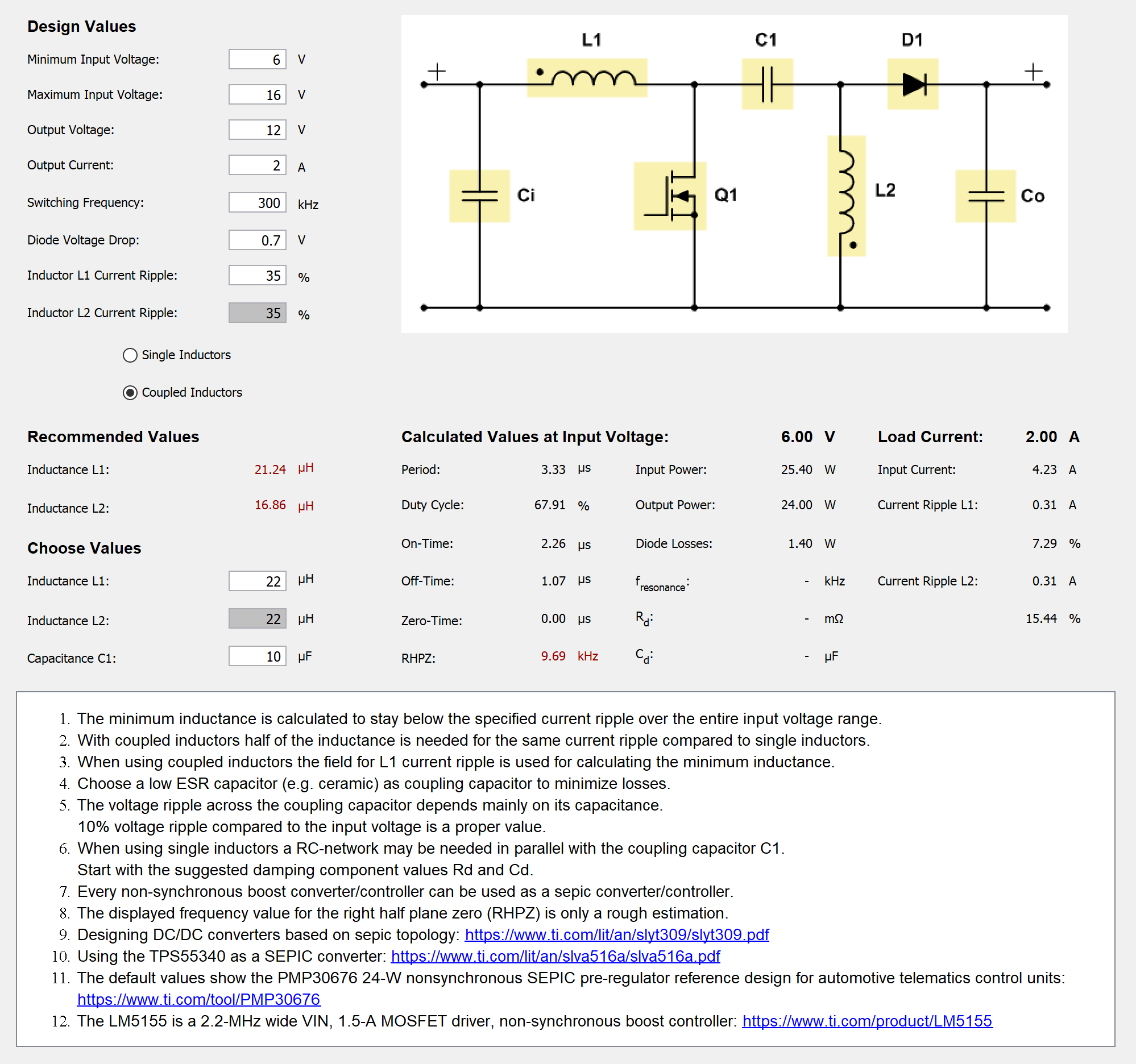
To start a power supply design with Power Stage Designer, first select a topology from the Topology menu. The window changes and displays the schematic of the selected topology with a set of input fields and various output values. After entering the parameters of the power supply specification, Power Stage Designer suggests a value for the output inductance to stay below the entered current ripple requirement. For isolated topologies, the tool also displays a recommendation for the transformer turns ratio (TTR) based on the selected maximum duty cycle and suggests a value for the magnetizing inductance. Users can enter values of their choice and evaluate their impact on voltage and current waveforms and other parameters like on-time, off-time, and duty cycle.
#SLVUBB49830 shows the main window of Power Stage Designer displaying supported topologies.
 Figure 1-1 Main
Window of Power Stage Designer Displaying Supported Topologies
 Figure 1-2 Topology
Window for SEPIC
Figure 1-2 Topology
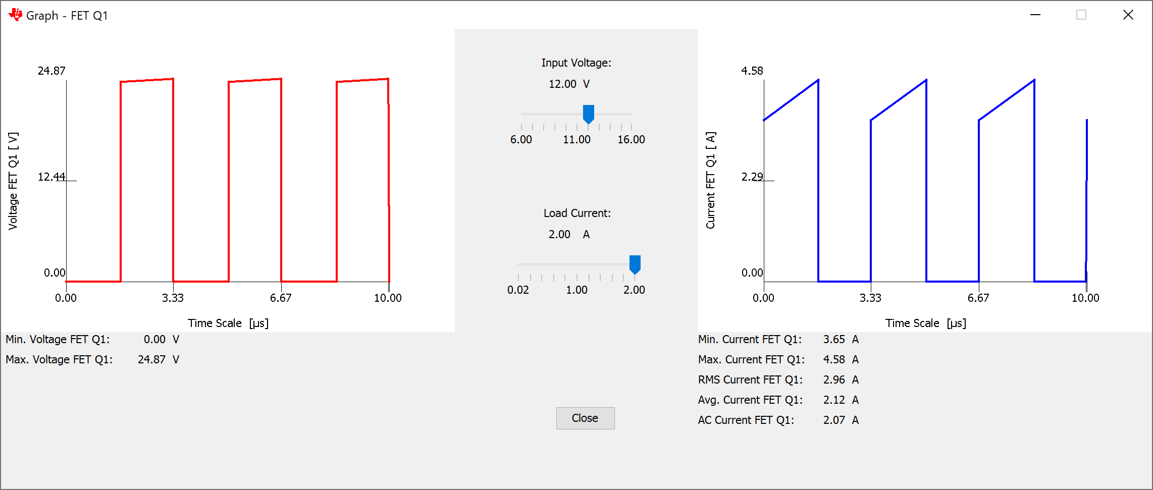
Window for SEPICAfter clicking on one of the yellow highlighted components in the schematic (see #SLVUBB42919), a new window displays the voltage and current waveforms for this specific component (see #SLVUBB45520). Additional information like the minimum and maximum voltage, minimum and maximum current, as well as root mean square (RMS), average, and AC values for the current is also provided in this window. The input voltage can be changed across the entire input voltage range with a slider. For most topologies the load current can be altered in the range of 1% to 100% of the entered output current with a second slider. Some topology models do not support such a wide load current range, thus the load current slider can be changed only in the range of 50% and 100%. The Quasi-resonant Flyback model uses a fixed output power as base for all calculations. That is why the load current slider is not available for this specific topology.
 Figure 1-3 Graph
Window for FET Q1 of a SEPIC Operating in CCM
Figure 1-3 Graph
Window for FET Q1 of a SEPIC Operating in CCMAll equations used for calculations are ideal, with the only exception that the forward voltage of rectifier and freewheeling diodes is considered. For a collection of the equations behind certain topologies, see the Power Topologies Handbook.