SLVUBB4B November 2017 – February 2023
- Abstract
- Trademarks
- 1 Topologies Window
- 2 FET Losses Calculator
- 3 Load Step Calculator
- 4 Capacitor Current Sharing Calculator
- 5 AC/DC Bulk Capacitor Calculator
- 6 RCD-Snubber Calculator for Flyback Converters
- 7 RC-Snubber Calculator
- 8 Output Voltage Resistor Divider
- 9 Dynamic Analog Output Voltage Scaling
- 10Dynamic Digital Output Voltage Scaling
- 11Unit Converter
-
12Loop Calculator
- 12.1 Inputs
- 12.2
Transfer Functions
- 12.2.1 Output Impedance Transfer Function
- 12.2.2 Transfer Function VMC Buck Power Stage
- 12.2.3 Transfer Function CMC Buck Power Stage
- 12.2.4 Transfer Function CMC Boost Power Stage
- 12.2.5 Transfer Function CMC Inverting Buck-Boost Power Stage
- 12.2.6 Transfer Function CMC Forward Power Stage
- 12.2.7 Transfer Function CMC Flyback Power Stage
- 12.2.8 Transfer Function Closed Loop
- 12.2.9 Transfer Function Isolated Type II Compensation Network With a Zener Clamp
- 12.2.10 Transfer Function Isolated Type II Compensation Network Without a Zener Clamp
- 13Filter Designer
- 14Additional Information
- 15Revision History
6 RCD-Snubber Calculator for Flyback Converters
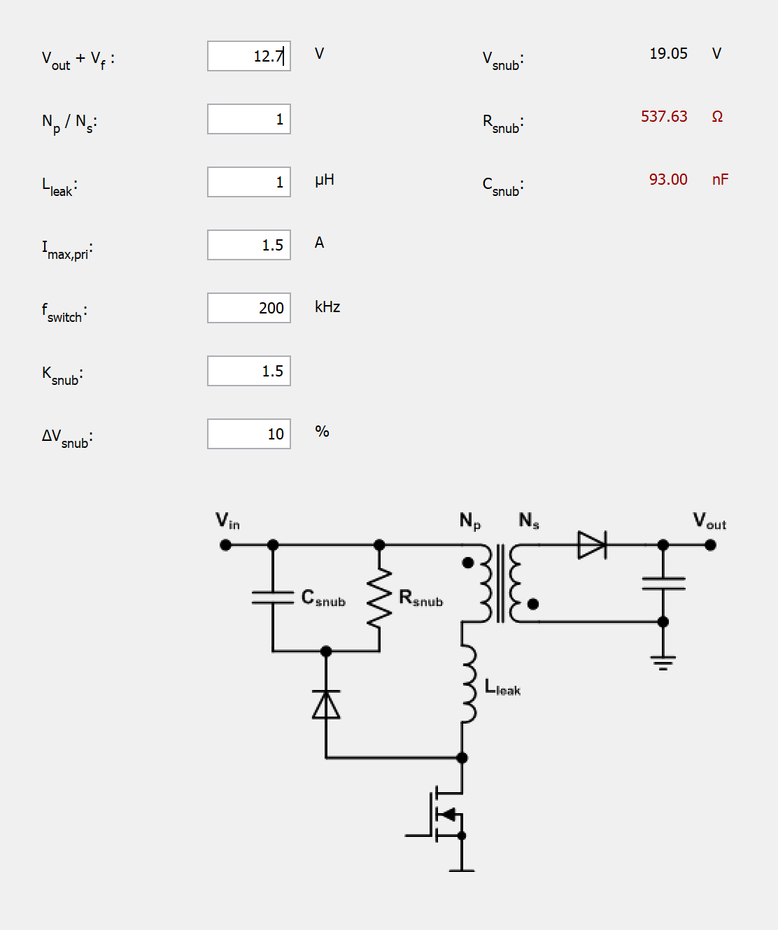
In Flyback converters the output voltage is reflected from the secondary to the primary side. Additionally, parasitics caused by the layout and the Flyback transformer leakage inductance can cause a voltage spike followed by ringing when the MOSFET is turning off. The voltage spike and the ringing can be limited by implementing an RCD-snubber circuit in parallel to the primary winding. The energy of the high-frequency ringing is dissipated in the RCD-network. The RCD-Snubber Calculator for Flyback converters in Power Stage Designer helps the designer choose the starting values for snubber resistor and capacitor based on the user’s inputs, which follow:
- Sum of output voltage and rectifier voltage
- Flyback transformer turns ratio
- Leakage inductance
- Maximum primary current
- Switching frequency
- Permitted voltage overshoot as a factor
- Snubber capacitor voltage ripple in percent
#SLVUBB42043 shows the RCD-Snubber Calculator for Flyback Converters window.
 Figure 6-1 RCD-Snubber Calculator for Flyback Converters Window
Vsnub is the reflected output voltage plus the permitted overshoot caused by transformer leakage inductance and switching node parasitics. Thus Ksnub has a value greater than 1. TI recommends a value of 1.5 for most applications, permitting 50% overshoot (see [1]). See #SLVUBB45069.
Starting Snubber resistance:
Starting Snubber capacitance: