SLVUBQ1A August 2020 – May 2021 TPS543620
- Trademarks
- 1Introduction
- 2Configurations and Modifications
-
3Test Setup and Results
- 3.1 Input/Output Connections
- 3.2 Efficiency
- 3.3 Output Voltage Regulation
- 3.4 Load Transient and Loop Response
- 3.5 Output Voltage Ripple
- 3.6 Input Voltage Ripple
- 3.7 Synchronizing to a Clock
- 3.8 Start-up and Shutdown with EN
- 3.9 Start-up and Shutdown with VIN
- 3.10 Start-up Into Pre-Bias
- 3.11 Hiccup Current Limit
- 3.12 Overvoltage Protection
- 3.13 Thermal Performance
- 4Board Layout
- 5Schematic and Bill of Materials
- 6Revision History
3.9 Start-up and Shutdown with VIN
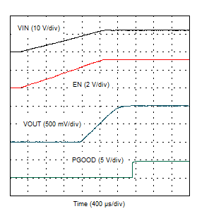
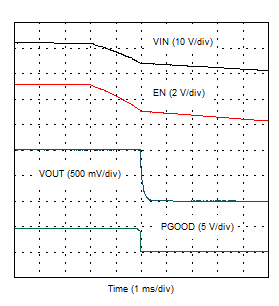
Figure 3-30 and Figure 3-31 show the start-up and shutdown waveforms for U2 with VIN. In Figure 3-30, the VIN voltage ramps up and output voltage ramps up after the input and EN pin voltages reach their respective UVLO threshold. In Figure 3-31, the VIN voltage ramps down and the TPS543620 shuts down when the input or EN pin voltage reach their respective UVLO threshold. The rate at which VIN ramps down changes as soon as the TPS543620 is disabled because it is no longer loading the input supply.
 Figure 3-30 U2 Start-up
with VIN – 0.3-Ω Load
 Figure 3-31 U2 Shutdown
with VIN – 0.3-Ω Load