SLVUBZ1 December 2020
4 PCB Layout
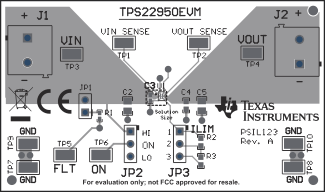
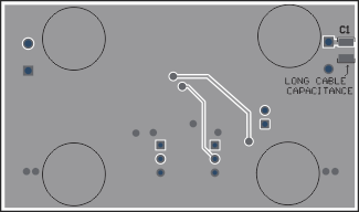
Figure 4-1 and Figure 4-2 show the PCB layout images.
 Figure 4-1 TPS22950EVM Top Layout
 Figure 4-2 TPS22950EVM Bottom Layout
SLVUBZ1 December 2020
Figure 4-1 and Figure 4-2 show the PCB layout images.
 Figure 4-1 TPS22950EVM Top Layout
 Figure 4-2 TPS22950EVM Bottom Layout