SLVUCA7 September 2021 TPS25859-Q1
4 Board Layout
Figure 4-1 and Figure 4-2 show the top and bottom assembly. Figure 4-3 and Figure 4-4 show the top side and bottom side 3D view. Figure 4-5 through Figure 4-8 show the layout images of the EVM.
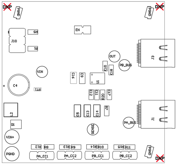 Figure 4-1 Top Side Assembly
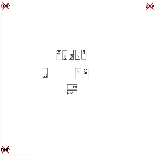 Figure 4-2 Bottom Side Assembly
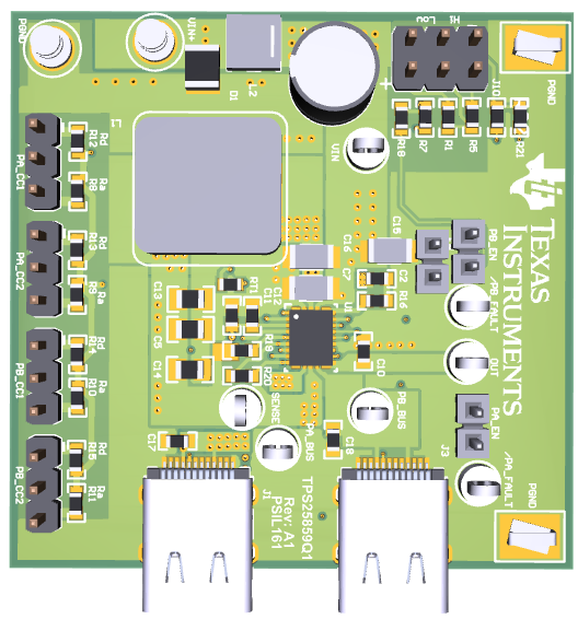 Figure 4-3 Top Side 3D View
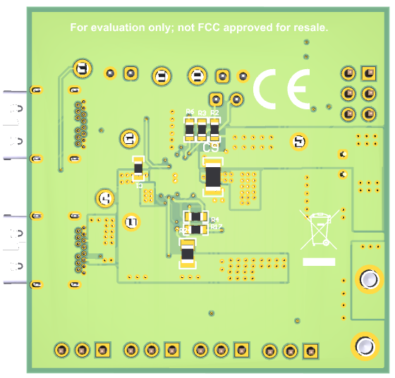 Figure 4-4 Bottom Side 3D
View
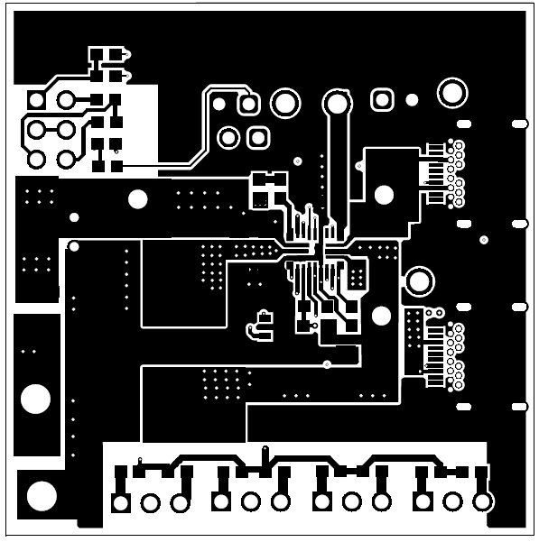 Figure 4-5 Top Layer Layout
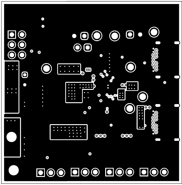 Figure 4-6 Mid-1 Layer Layout
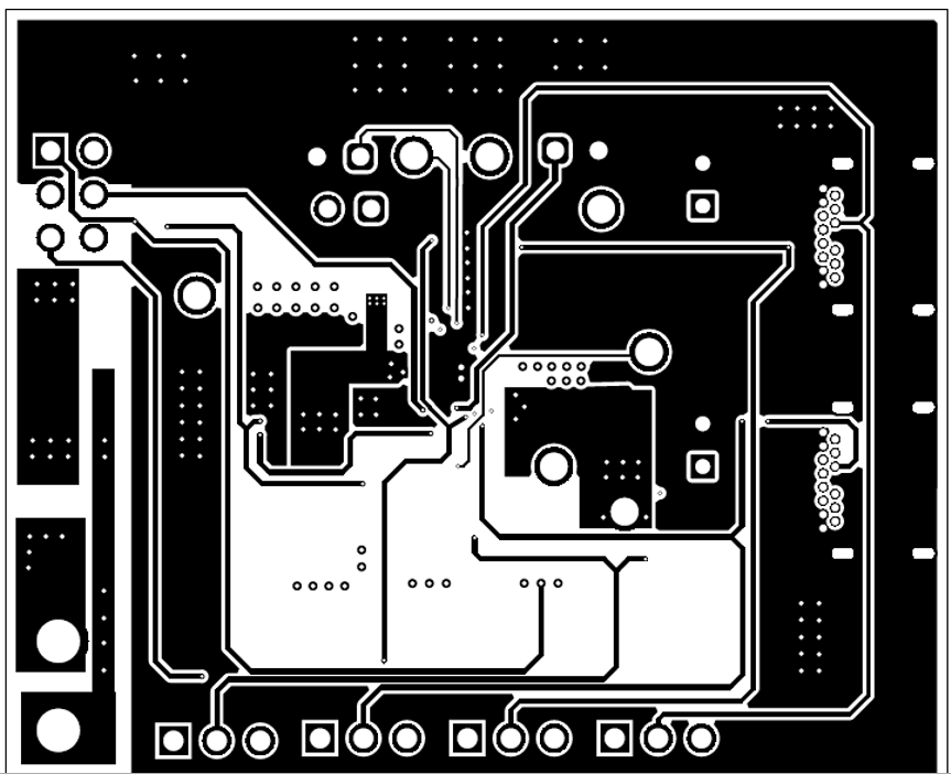 Figure 4-7 Mid-2 Layer Layout
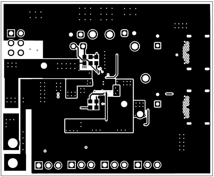 Figure 4-8 Bottom Layer
Layout