SLVUCF4 August 2022
PRODUCTION DATA
3.1 Parallel Configuration Results
The results shown in below were observed using the TPS7H2221EVM in its default parallel configuration with VIN = 3.3 V.
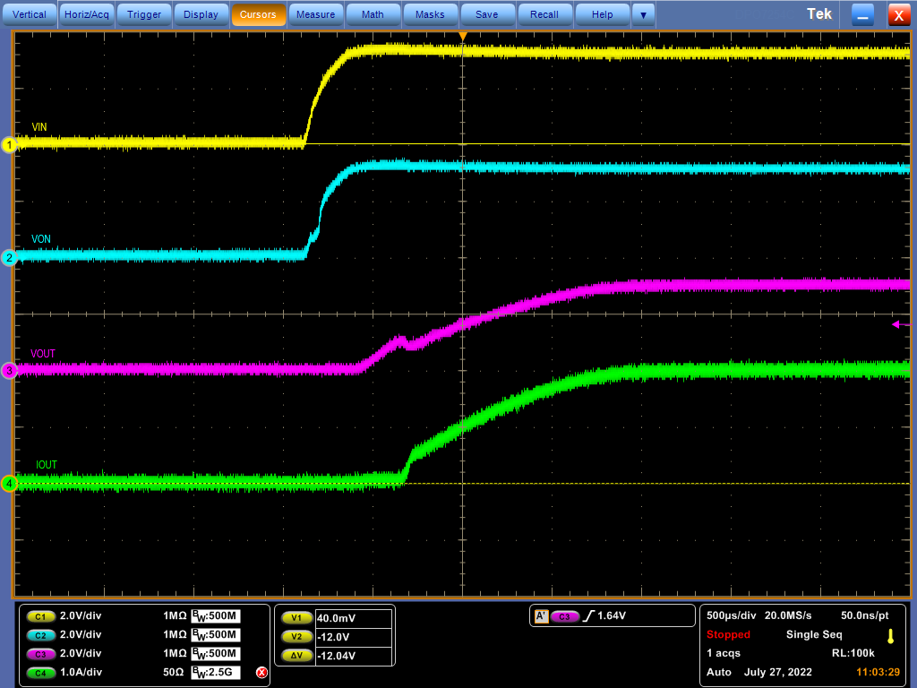
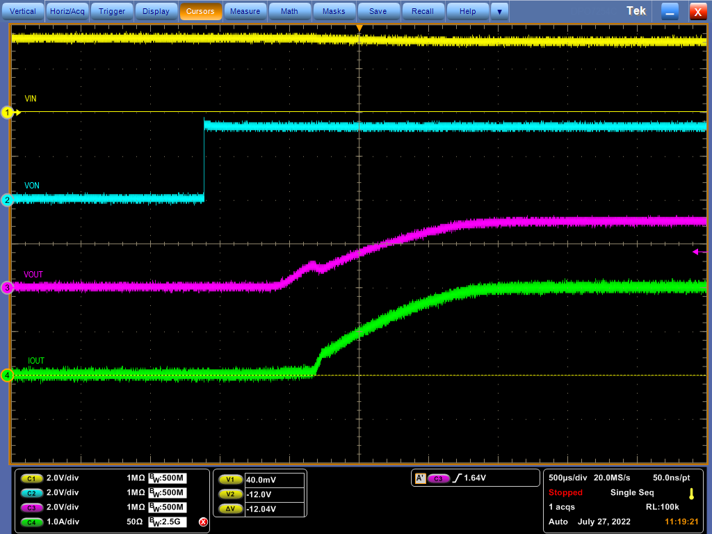
Startup Tests
When VON < VIL, the device connects a Smart Pull Down (typically 491 kOhms) to the ON pin to prevent it from floating until system sequencing is complete. Once VON is driven > VIH, the Smart Pull Down is disconnected.
By default, the ON pin is tied to VIN on the EVM via R2 so that the user can utilize the jumpers (JP2 or JP7) without leaving the ON pin floating. If the jumpers are not being utilized, it is typically recommended to remove R2 and enable the device by applying an external signal to the ON pin via J6 or TP5 once VIN is HIGH for cleaner startup.
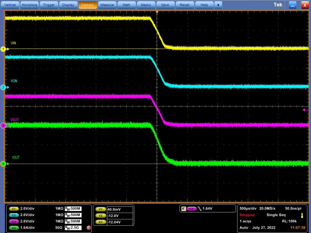
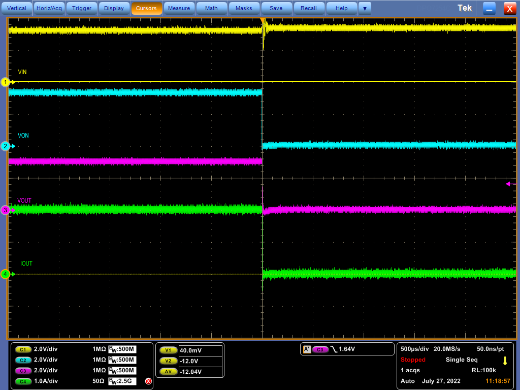
Shutdown Tests
Quick Output Discharge (QOD) Tests
The Quick Output Discharge (QOD) feature of the TPS7H2221-SEP is controlled by the voltage sensed at the ON pin. When VON > VIH, VOUT follows VIN. When VON < VIL, the output is discharged to GND via the QOD pin and RQOD (if desired). If the QOD pin is left open, then VOUT will be left floating when VON < VIL and it will discharge through the load or board parasitics.
In the Shutdown Tests section above, the scope shots show the difference in VOUT behavior when VON is tied to VIN versus when it is set LOW using an external signal. In the first case, VOUT simply follows VIN as it falls because VON > VIH. In the second case, VOUT is quickly discharged by the load and QOD because VON < VIL, which is preferred.
The results shown in this section focus on configurations where IOUT = 0A so that the impact of different QOD resistances on VOUT fall time can be more easily observed. If a higher load is present, it will typically be the dominant factor in VOUT fall time.
To calculate VOUT fall time for devices in parallel configuration, the total RQOD will be RQOD1 || RQOD2 and the total COUT will be COUT1 + COUT2.
Figure 3-5 Test Conditions: External signal applied to ON, IOUT = 0A, all QOD jumpers left open
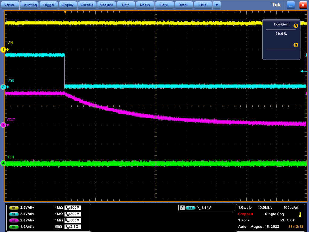 Figure 3-5 VOUT Fall Time: RQOD=OPEN
Figure 3-6 Test Conditions: External signal applied to ON, IOUT = 0A, JP4 and JP9 shunted
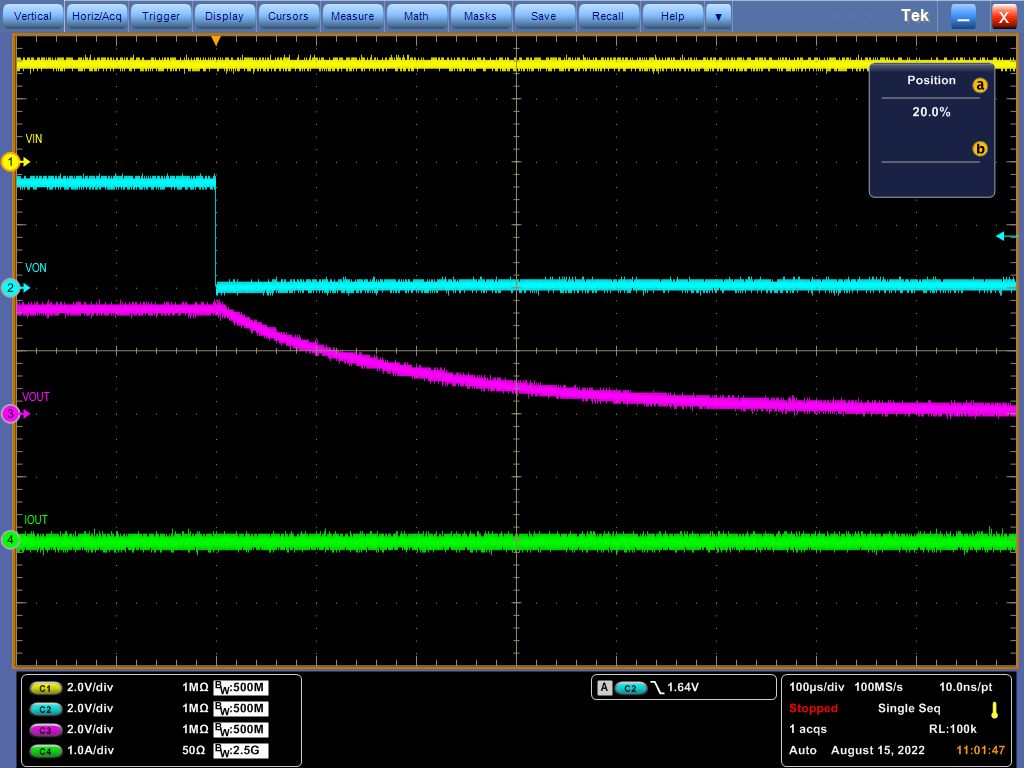 Figure 3-6 VOUT Fall Time: RQOD=1 kOhms
Figure 3-7 Test Conditions: External signal applied to ON, IOUT = 0A, JP5 and JP10 shunted
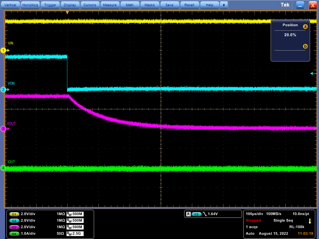 Figure 3-7 VOUT Fall Time: RQOD=500 Ohms
Figure 3-8 Test Conditions: External signal applied to ON, IOUT = 0A, JP3 and JP8 shunted
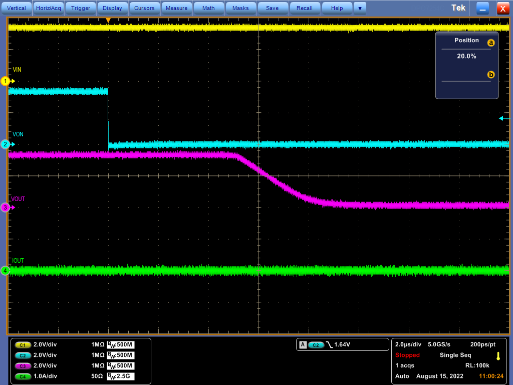 Figure 3-8 VOUT Fall Time: QOD tied to VOUT