SLWS230E September 2011 – December 2015 TRF3765
PRODUCTION DATA.
- 1 Features
- 2 Applications
- 3 Description
- 4 Revision History
- 5 Pin Configuration and Functions
- 6 Specifications
- 7 Detailed Description
- 8 Application and Implementation
- 9 Power Supply Recommendations
- 10Layout
- 11Device and Documentation Support
- 12Mechanical, Packaging, and Orderable Information
6 Specifications
6.1 Absolute Maximum Ratings
Over operating free-air temperature range (unless otherwise noted).(1)| MIN | MAX | UNIT | ||
|---|---|---|---|---|
| Supply voltage (2) | All VCC pins except VCC_TK | –0.3 | 3.6 | V |
| VCC_TK | –0.3 | 5.5 | ||
| Digital I/O voltage | –0.3 | VI + 0.5 | V | |
| Operating virtual junction temperature, TJ | –40 | 150 | °C | |
| Operating ambient temperature, TA | –40 | 85 | °C | |
| Storage temperature, Tstg | –40 | 150 | °C | |
(1) Stresses beyond those listed under Absolute Maximum Ratings may cause permanent damage to the device. These are stress ratings only, which do not imply functional operation of the device at these or any other conditions beyond those indicated under Recommended Operating Conditions. Exposure to absolute-maximum-rated conditions for extended periods may affect device reliability.
(2) All voltage values are with respect to network ground pin.
6.2 ESD Ratings
| VALUE | UNIT | |||
|---|---|---|---|---|
| V(ESD) | Electrostatic discharge | Human body model (HBM), per ANSI/ESDA/JEDEC JS-001(1) | ±1000 | V |
| Charged device model (CDM), per JEDEC specification JESD22-C101(2) | ±1500 | |||
(1) JEDEC document JEP155 states that 500-V HBM allows safe manufacturing with a standard ESD control process.
(2) JEDEC document JEP157 states that 250-V CDM allows safe manufacturing with a standard ESD control process.
6.3 Recommended Operating Conditions
Over operating free-air temperature range (unless otherwise noted).| MIN | NOM | MAX | UNIT | ||
|---|---|---|---|---|---|
| VCC | Power-supply voltage | 3 | 3.3 | 3.6 | V |
| VCC_TK | 3.3-V to 5.5-V power-supply voltage | 3 | 3.3 | 5.5 | V |
| TA | Operating ambient temperature | –40 | 85 | °C | |
| TJ | Operating virtual junction temperature | –40 | 150 | °C | |
6.4 Thermal Information
| THERMAL METRIC(1) | TRF3765 | UNIT | |
|---|---|---|---|
| RHB (VQFN) | |||
| 32 PINS | |||
| RθJA | Junction-to-ambient thermal resistance | 31.6 | °C/W |
| RθJCtop | Junction-to-case (top) thermal resistance | 21.6 | °C/W |
| RθJB | Junction-to-board thermal resistance | 5.6 | °C/W |
| ψJT | Junction-to-top characterization parameter | 0.3 | °C/W |
| ψJB | Junction-to-board characterization parameter | 5.5 | °C/W |
| RθJCbot | Junction-to-case (bottom) thermal resistance | 1.1 | °C/W |
(1) For more information about traditional and new thermal metrics, see the Semiconductor and IC Package Thermal Metrics application report, SPRA953.
6.5 Electrical Characteristics
At TA = 25°C and power supply = 3.3 V, unless otherwise noted.| PARAMETERS | TEST CONDITIONS | MIN | TYP | MAX | UNIT | ||
|---|---|---|---|---|---|---|---|
| DC PARAMETERS | |||||||
| ICC | Total supply current | Internal VCO, 1 output buffer on, divide-by-1 | 115 | mA | |||
| Internal VCO, 4 output buffers on, divide-by-1 | 190 | ||||||
| Internal VCO, 1 output buffer on, divide-by-8 | 120 | ||||||
| Internal VCO, 4 output buffers on, divide-by-8 | 182 | ||||||
| External VCO mode, 1 output buffer on, divide-by-1 | 89 | ||||||
| DIGITAL INTERFACE | |||||||
| VIH | High-level input voltage | 2 | 3.3 | V | |||
| VIL | Low-level input voltage | 0 | 0.8 | ||||
| VOH | High-level output voltage | Referenced to VCC_DIG | 0.8 × VCC | ||||
| VOL | Low-level output voltage | Referenced to VCC_DIG | 0.2 × VCC | ||||
| REFERENCE OSCILLATOR PARAMETERS | |||||||
| fREF | Reference frequency | 0.5(6) | 350(6) | MHz | |||
| Reference input sensitivity | 0.2 | 3.3 | VPP | ||||
| Reference input impedance | Parallel capacitance, 10 MHz | 2 | pF | ||||
| Parallel resistance, 10 MHz | 2500 | Ω | |||||
| PLL | |||||||
| fPFD | PFD frequency | 0.5 | 65(1) | MHz | |||
| ICP_OUT | Charge pump current | 4WI programmable; ICP[4..0] = 00000(2) | 1.94 | mA | |||
| In-band normalized phase noise floor | Integer mode | –221 | dBc/Hz | ||||
| INTERNAL VCO | |||||||
| fVCO | VCO frequency range | Divide-by-1 | 2400 | 4800 | MHz | ||
| KV | VCO gain | VCP = 1 V | –65 | MHz/V | |||
| VCO free-running phase noise, fVCO = 2650 MHz |
VCC_TK = 3.3 V | At 10 kHz | –82 | dBc/Hz | |||
| At 100 kHz | –110 | ||||||
| At 1 MHz | –130 | ||||||
| At 10 MHz | –149 | ||||||
| At 40 MHz | –155 | ||||||
| VCC_TK = 5 V | At 10 kHz | –89 | dBc/Hz | ||||
| At 100 kHz | –113 | ||||||
| At 1 MHz | –133 | ||||||
| At 10 MHz | –151 | ||||||
| At 40 MHz | –156 | ||||||
| CLOSED-LOOP PLL/VCO | |||||||
| Integrated RMS jitter(3) | Fractional mode, fOUT = 2.6 GHz, fPFD = 30.72 MHz(4) | 0.36 | ps | ||||
| Integer mode, fOUT = 2.6 GHz, fPFD = 1.6 MHz | 0.52 | ||||||
| RF OUTPUT/INPUT | |||||||
| fOUT | Output frequency range | Divide-by-1 | 2400 | 4800 | MHz | ||
| Divide-by-2 | 1200 | 2400 | |||||
| Divide-by-4 | 600 | 1200 | |||||
| Divide-by-8 | 300 | 600 | |||||
| PLO | Output power(5) | Differential, divide-by-1, one output buffer on, maximum BUFOUT_BIAS | 6.5 | dBm | |||
| External VCO input maximum frequency | 20-dB gain loss, VCO pass-through, no PLL | 9000 | MHz | ||||
| External VCO input minimum frequency | 20-dB gain loss, VCO pass-through, no PLL, divide-by-1 | 15 | MHz | ||||
| External VCO input level | 0 | dBm | |||||
(1) See Application Information for discussion on PFD frequency selection and calibration logic frequency limitations.
(2) See 4WI Register Descriptions for all possible programmable charge pump currents.
(3) Integrated from 1 kHz to 10 MHz.
(4) See Application Information for information on loop filter characteristics.
(5) See Application Information for external output buffers details.
(6) See Application Information for discussion of VCO calibration clock limitations on reference clock frequency.
6.6 4WI Timing: Write Operation
See Figure 1.| MIN | MAX | UNIT | ||
|---|---|---|---|---|
| th | Hold time, data to clock | 20 | ns | |
| tsu1 | Setup time, data to clock | 20 | ns | |
| t(CH) | Clock low duration | 20 | ns | |
| t(CL) | Clock high duration | 20 | ns | |
| tsu2 | Setup time, clock to enable | 20 | ns | |
| t(CLK) | Clock period | 50 | ns | |
| tw | Enable time | 50 | ns | |
| tsu3 | Setup time, latch to data | 70 | ns | |
6.7 Readback 4WI Timing
See Figure 2.| MIN | MAX | UNIT | ||
|---|---|---|---|---|
| th | Hold time, data to clock | 20 | ns | |
| tsu1 | Setup time, data to clock | 20 | ns | |
| t(CH) | Clock low duration | 20 | ns | |
| t(CL) | Clock high duration | 20 | ns | |
| tsu2 | Setup time, clock to enable | 20 | ns | |
| tsu3 | Setup time, enable to Readback clock | 20 | ns | |
| td | Delay time, clock to Readback data output | 10 | ns | |
| tw(1) | Enable time | 50 | ns | |
| t(CLK) | Clock period | 50 | ns | |
(1) Equals Clock period
 Figure 1. 4WI Timing Diagram
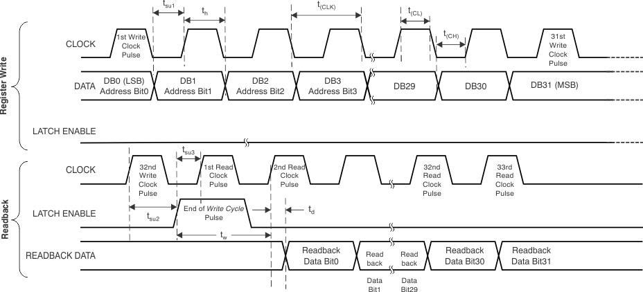 Figure 2. 4WI Readback Timing Diagram
6.8 Typical Characteristics
Table 1. Table of Graphs
| GRAPH NAME | FIGURE NO. | |
| Open-Loop Phase Noise | vs Temperature(1) | Figure 3, Figure 4, Figure 5, Figure 6 |
| Open-Loop Phase Noise | vs Voltage(1) | Figure 7, Figure 8, Figure 9, Figure 10 |
| Open-Loop Phase Noise | vs Temperature(1)(2) | Figure 11, Figure 12, Figure 13, Figure 14 |
| Open-Loop Phase Noise | vs Voltage(1)(2) | Figure 15, Figure 16, Figure 17, Figure 18 |
| Closed-Loop Phase Noise | vs Temperature(3) | Figure 19, Figure 20, Figure 21, Figure 22, Figure 23, Figure 24, Figure 25 |
| Closed-Loop Phase Noise | vs Temperature(2)(3) | Figure 26, Figure 27, Figure 28, Figure 29, Figure 30, Figure 31, Figure 32 |
| Closed-Loop Phase Noise | vs Divide Ratio(3) | Figure 33 |
| Closed-Loop Phase Noise | vs Divide Ratio(2)(3) | Figure 34 |
| Closed-Loop Phase Noise | vs Temperature(4) | Figure 35, Figure 36, Figure 37, Figure 38, Figure 39, Figure 40, Figure 41 |
| Closed-Loop Phase Noise | vs Temperature(2)(4) | Figure 42, Figure 43, Figure 44, Figure 45, Figure 46, Figure 47, Figure 48 |
| Closed-Loop Phase Noise | vs Divide Ratio(4) | Figure 49 |
| Closed-Loop Phase Noise | vs Divide Ratio(2)(4) | Figure 50 |
| PFD Spurs | vs Temperature(4) | Figure 51 |
| Multiples of PFD Spurs(4) | Figure 52, Figure 53, Figure 54 | |
| Multiples of PFD Spurs(4)(5) | Figure 55 | |
| Fractional Spurs | vs LO Divider(3) | Figure 56 |
| Fractional Spurs | vs RF Divider and Prescaler(3) | Figure 57 |
| Fractional Spurs | vs Temperature(3) | Figure 58 |
| Multiples of PFD Spurs(3) | Figure 59 | |
| LO Harmonics(4) | Figure 60 | |
| Output Power with Multiple Buffers(4) | Figure 61, Figure 62 | |
| Output Power | vs Output Port(4) | Figure 63 |
| Output Power | vs Buffer Bias(4) | Figure 64 |
| VCO Gain (Kv) | vs Frequency | Figure 65 |
(1) VCO_TRIM = 32, VTUNE_IN = 1.1 V, CP_TRISTATE = 3 (3-state), and CAL_BYPASS = On.
(2) VCO_BIAS = 600 µA.
(3) Reference frequency = 61.44 MHz; PFD frequency = 30.72 MHz.
(4) Reference frequency = 40 MHz; PFD frequency = 1.6 MHz.
(5) Performance change at frequencies above 1500 MHz results from PLL_DIV_SEL changing from divide-by-1 to divide-by-2.
At TA = 25°C, VCC = 3.3 V, VCC_TK = 3.3 V, LO1_OUTP (single-ended), PWD_BUFF2,3,4 = off, VCO_BIAS = 400 µA; BUFOUT_BIAS = 600 µA, all other registers set per recommended programming in Serial Programming Interface Register Definitions, and standard operating condition, unless otherwise noted.
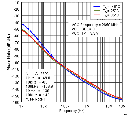 Figure 3. Open-Loop Phase Noise vs Temperature
(VCO_SEL = 0 and VCC_TK = 3.3 V)
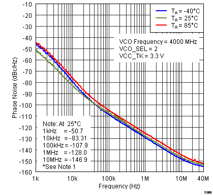 Figure 5. Open-Loop Phase Noise vs Temperature
(VCO_SEL = 2 and VCC_TK = 3.3 V)
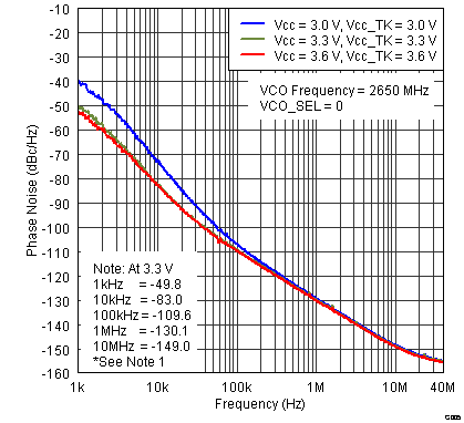 Figure 7. Open-Loop Phase Noise vs voltage
(VCO_SEL = 0)
 Figure 9. Open-Loop Phase Noise vs Voltage
(VCO_SEL = 2)
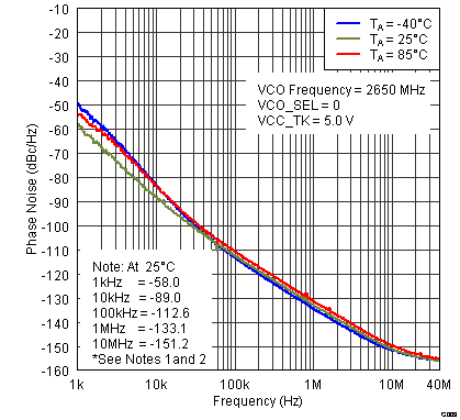 Figure 11. Open-Loop Phase Noise vs Temperature
(VCO_SEL = 0 and VCC_TK = 5 V)
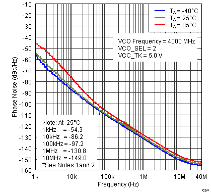 Figure 13. Open-Loop Phase Noise vs Temperature
(VCO_SEL = 2 and VCC_TK = 5 V)
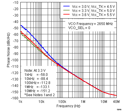 Figure 15. Open-Loop Phase Noise vs Voltage
(VCO_SEL = 0)
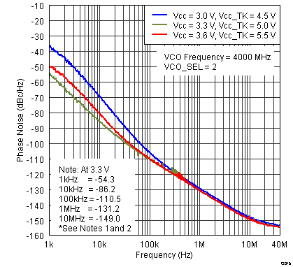 Figure 17. Open-Loop Phase Noise vs Voltage
(VCO_SEL = 2)
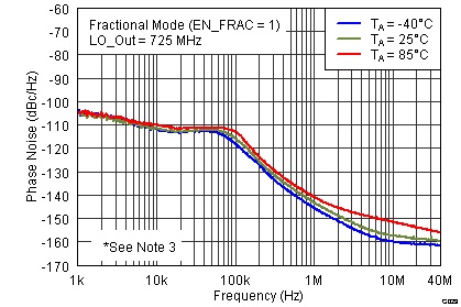 Figure 19. Closed-Loop Phase Noise vs Temperature
(725 MHz, VCC_TK = 3.3 V, Fractional Mode)
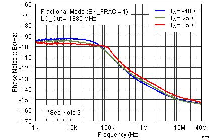 Figure 21. Closed-Loop Phase Noise vs Temperature
(1880 MHz, VCC_TK = 3.3 V, Fractional Mode)
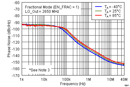 Figure 23. Closed-Loop Phase Noise vs Temperature
(2650 MHz, VCC_TK = 3.3 V, Fractional Mode)
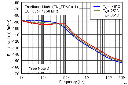 Figure 25. Closed-Loop Phase Noise vs Temperature
(4750 MHz, VCC_TK = 3.3 V, Fractional Mode)
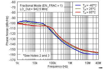 Figure 27. Closed-Loop Phase Noise vs Temperature
(942.5 MHz, VCC_TK = 5 V, Fractional Mode)
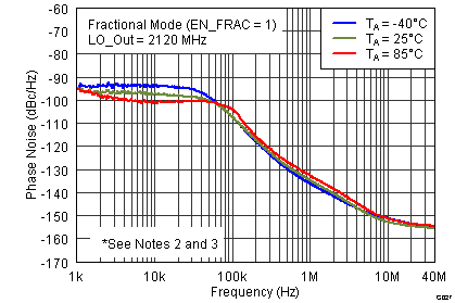 Figure 29. Closed-Loop Phase Noise vs Temperature
(2120 MHz, VCC_TK = 5 V, Fractional Mode)
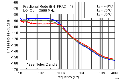 Figure 31. Closed-Loop Phase Noise vs Temperature
(3500 MHz, VCC_TK = 5 V, Fractional Mode)
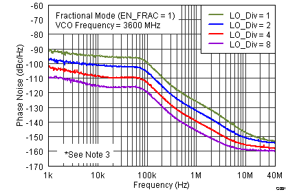 Figure 33. Closed-Loop Phase Noise vs Divide Ratio
(VCC_TK = 3.3 V, Fractional Mode)
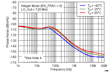 Figure 35. Closed-Loop Phase Noise vs Temperature
(728 MHz, VCC_TK = 3.3 V, Integer Mode)
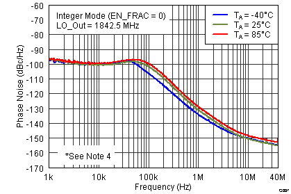 Figure 37. Closed-Loop Phase Noise vs Temperature
(1842.5 MHz, VCC_TK = 3.3 V, Integer Mode)
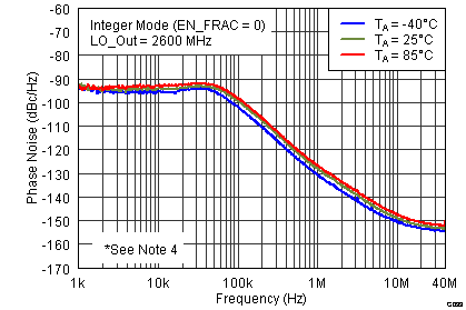 Figure 39. Closed-Loop Phase Noise vs Temperature
(2600 MHz, VCC_TK = 3.3 V, Integer Mode)
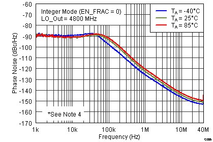 Figure 41. Closed-Loop Phase Noise vs Temperature
(4800 MHz, VCC_TK = 3.3 V, Integer Mode)
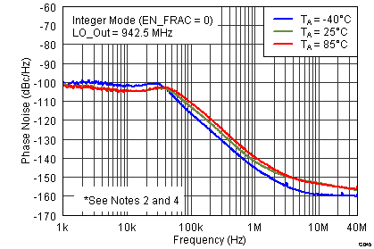 Figure 43. Closed-Loop Phase Noise vs Temperature
(942.5 MHz, VCC_TK = 5 V, Integer Mode)
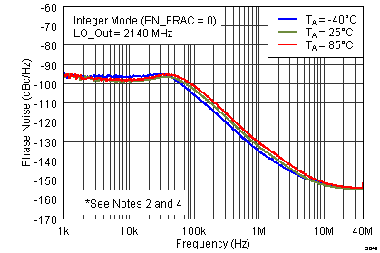 Figure 45. Closed-Loop Phase Noise vs Temperature
(2140 MHz, VCC_TK = 5 V, Integer Mode)
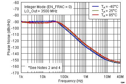 Figure 47. Closed-Loop Phase Noise vs Temperature
(3500 MHz, VCC_TK = 5 V, Integer Mode)
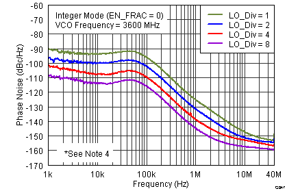 Figure 49. Closed-Loop Phase Noise vs Divide Ratio
(VCC_TK = 3.3 V, Integer Mode)
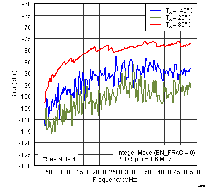 Figure 51. PFD Spurs vs Temperature
(Integer Mode)
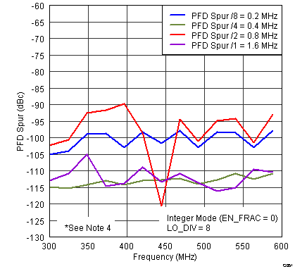 Figure 53. Multiples of PFD Spurs
(LO_DIV = 8, Integer Mode)
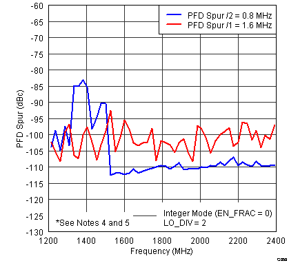 Figure 55. Multiples of PFD Spurs
(LO_DIV = 2, Integer Mode)
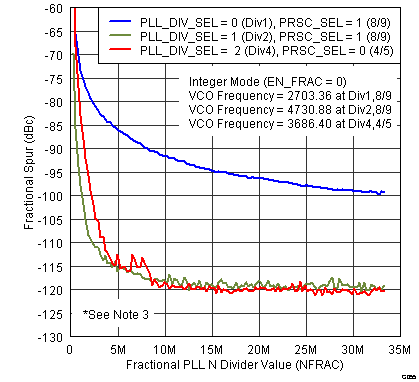 Figure 57. Fractional Spurs vs RF Divider and Prescaler
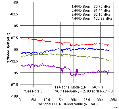 Figure 59. Multiples of PFD Spurs
(Fractional Mode)
 Figure 61. Output Power on LO1_OUTP With Multiple Buffers
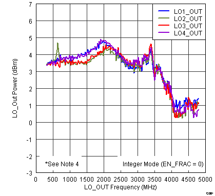 Figure 63. Output Power vs Output Port
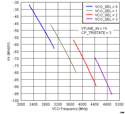 Figure 65. VCO Gain (Kv) vs Frequency
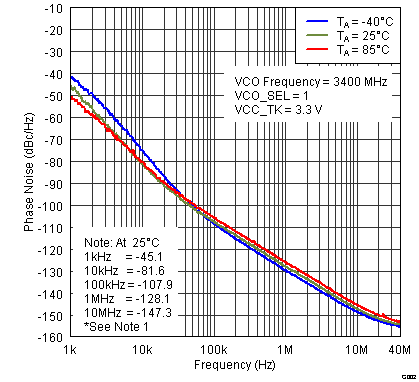 Figure 4. Open-Loop Phase Noise vs Temperature
(VCO_SEL = 1 and VCC_TK = 3.3 V)
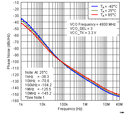 Figure 6. Open-Loop Phase Noise vs Temperature
(VCO_SEL = 3 and VCC_TK = 3.3 V)
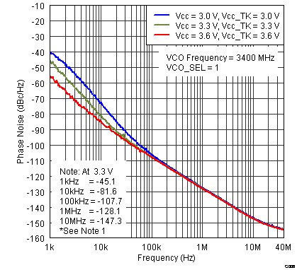 Figure 8. Open-Loop Phase Noise vs Voltage
(VCO_SEL = 1)
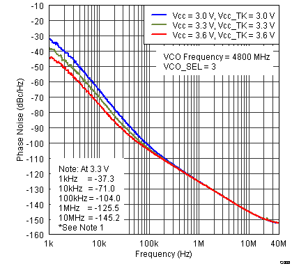 Figure 10. Open-Loop Phase Noise vs Voltage
(VCO_SEL = 3)
 Figure 12. Open-Loop Phase Noise vs Temperature
(VCO_SEL = 1 and VCC_TK = 5 V)
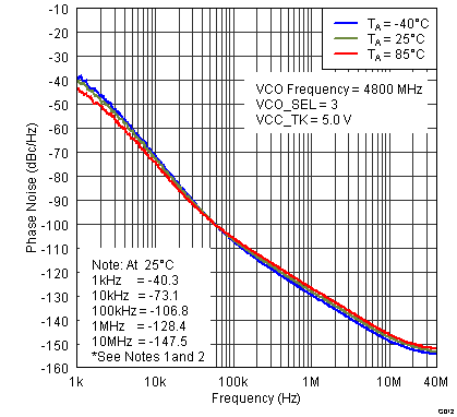 Figure 14. Open-Loop Phase Noise vs Temperature
(VCO_SEL = 3 and VCC_TK = 5 V)
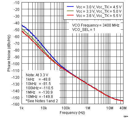 Figure 16. Open-Loop Phase Noise vs Voltage
(VCO_SEL = 1)
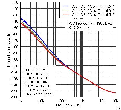 Figure 18. Open-Loop Phase Noise vs Voltage
(VCO_SEL = 3)
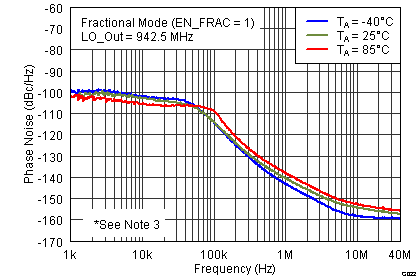 Figure 20. Closed-Loop Phase NoisE vs Temperature
(942.5 MHz, VCC_TK = 3.3 V, Fractional Mode)
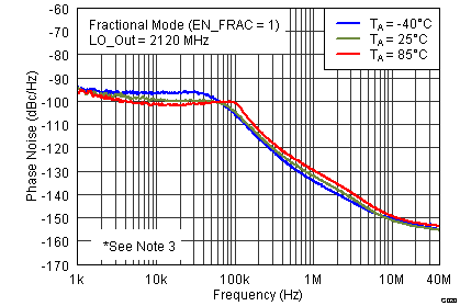 Figure 22. Closed-Loop Phase Noise vs Temperature
(2120 MHz, VCC_TK = 3.3 V, Fractional Mode)
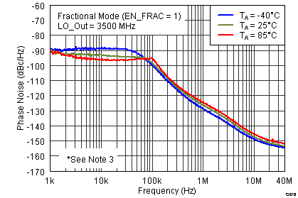 Figure 24. Closed-Loop Phase Noise vs Temperature
(3500 MHz, VCC_TK = 3.3 V, Fractional Mode)
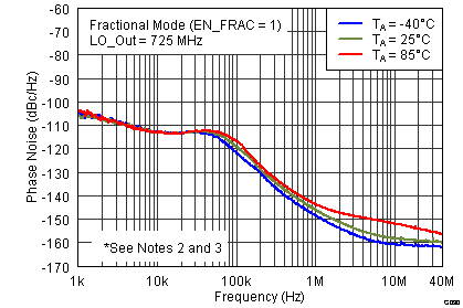 Figure 26. Closed-Loop Phase Noise vs Temperature
(725 MHz, VCC_TK = 5 V, Fractional Mode)
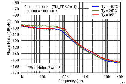 Figure 28. Closed-Loop Phase Noise vs Temperature
(1880 MHz, VCC_TK = 5 V, Fractional Mode)
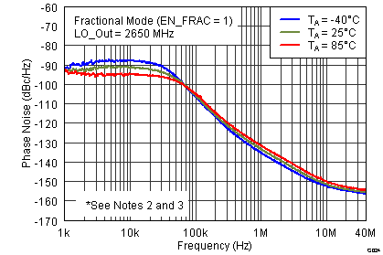 Figure 30. Closed-Loop Phase Noise vs Temperature
(2650 MHz, VCC_TK = 5 V, Fractional Mode)
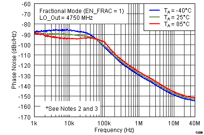 Figure 32. Closed-Loop Phase Noise vs Temperature
(4750 MHz, VCC_TK = 5 V, Fractional Mode)
 Figure 34. Closed-Loop Phase Noise vs Divide Ratio
(VCC_TK = 5 V, Fractional Mode)
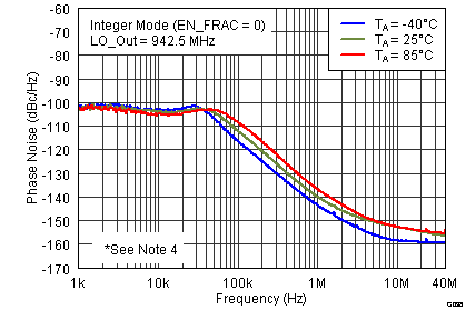 Figure 36. Closed-Loop Phase Noise vs Temperature
(942.5 MHz, VCC_TK = 3.3 V, Integer Mode)
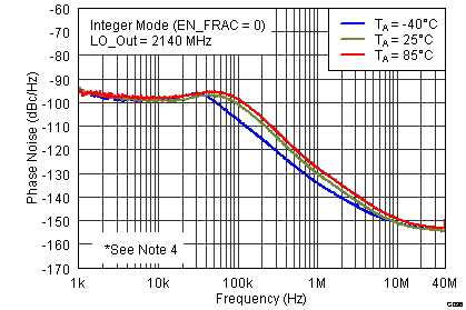 Figure 38. Closed-Loop Phase Noise vs Temperature
(2140 MHz, VCC_TK = 3.3 V, Integer Mode)
 Figure 40. Closed-Loop Phase Noise vs Temperature
(3500 MHz, VCC_TK = 3.3 V, Integer Mode)
 Figure 42. Closed-Loop Phase Noise vs Temperature
(728 MHz, VCC_TK = 5 V, Integer Mode)
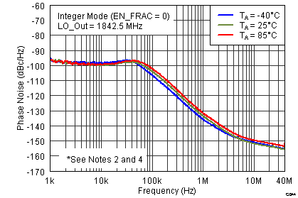 Figure 44. Closed-Loop Phase Noise vs Temperature
(1842.5 MHz, VCC_TK = 5 V, Integer Mode)
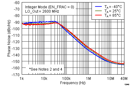 Figure 46. Closed-Loop Phase Noise vs Temperature
(2600 MHz, VCC_TK = 5 V, Integer Mode)
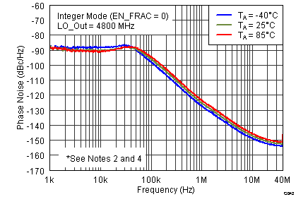 Figure 48. Closed-Loop Phase Noise vs Temperature
(4800 MHz, VCC_TK = 5 V, Integer Mode)
 Figure 50. Closed-Loop Phase Noise vs Divide Ratio
(VCC_TK = 5 V, Integer Mode)
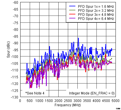 Figure 52. Multiples of PFD Spurs
(Integer Mode)
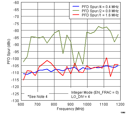 Figure 54. Multiples of PFD spurs
(LO_DIV = 4, Integer Mode)
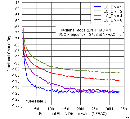 Figure 56. Fractional Spurs vs LO divider
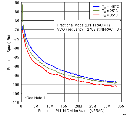 Figure 58. Fractional Spurs vs Temperature
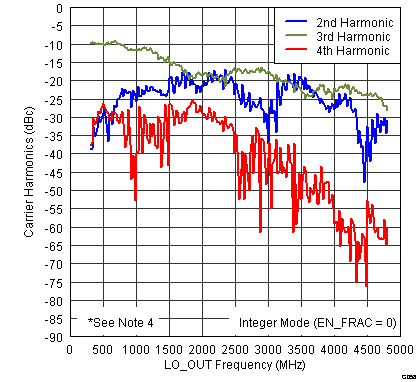 Figure 60. LO Harmonics
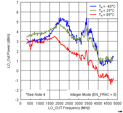 Figure 62. Output Power With Multiple Buffers
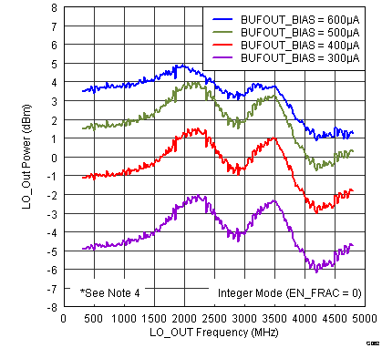 Figure 64. Output Power vs Buffer Bias
 Figure 3. Open-Loop Phase Noise vs Temperature
 (VCO_SEL = 0 and VCC_TK = 3.3 V)
 Figure 5. Open-Loop Phase Noise vs Temperature
(VCO_SEL = 2 and VCC_TK = 3.3 V)
 Figure 7. Open-Loop Phase Noise vs voltage
(VCO_SEL = 0)
 Figure 9. Open-Loop Phase Noise vs Voltage
(VCO_SEL = 2)
 Figure 11. Open-Loop Phase Noise vs Temperature
(VCO_SEL = 0 and VCC_TK = 5 V)
 Figure 13. Open-Loop Phase Noise vs Temperature
(VCO_SEL = 2 and VCC_TK = 5 V)
 Figure 15. Open-Loop Phase Noise vs Voltage
(VCO_SEL = 0)
 Figure 17. Open-Loop Phase Noise vs Voltage
(VCO_SEL = 2)

(725 MHz, VCC_TK = 3.3 V, Fractional Mode)

(1880 MHz, VCC_TK = 3.3 V, Fractional Mode)

(2650 MHz, VCC_TK = 3.3 V, Fractional Mode)

(4750 MHz, VCC_TK = 3.3 V, Fractional Mode)

(942.5 MHz, VCC_TK = 5 V, Fractional Mode)

(2120 MHz, VCC_TK = 5 V, Fractional Mode)

(3500 MHz, VCC_TK = 5 V, Fractional Mode)

(VCC_TK = 3.3 V, Fractional Mode)

(728 MHz, VCC_TK = 3.3 V, Integer Mode)

(1842.5 MHz, VCC_TK = 3.3 V, Integer Mode)

(2600 MHz, VCC_TK = 3.3 V, Integer Mode)

(4800 MHz, VCC_TK = 3.3 V, Integer Mode)

(942.5 MHz, VCC_TK = 5 V, Integer Mode)

(2140 MHz, VCC_TK = 5 V, Integer Mode)

(3500 MHz, VCC_TK = 5 V, Integer Mode)

(VCC_TK = 3.3 V, Integer Mode)
 Figure 51. PFD Spurs vs Temperature
(Integer Mode)
 Figure 53. Multiples of PFD Spurs
(LO_DIV = 8, Integer Mode)
 Figure 55. Multiples of PFD Spurs
(LO_DIV = 2, Integer Mode)
 Figure 57. Fractional Spurs vs RF Divider and Prescaler
 Figure 59. Multiples of PFD Spurs
(Fractional Mode)
 Figure 61. Output Power on LO1_OUTP With Multiple Buffers
 Figure 63. Output Power vs Output Port
 Figure 65. VCO Gain (Kv) vs Frequency
 Figure 4. Open-Loop Phase Noise vs Temperature
(VCO_SEL = 1 and VCC_TK = 3.3 V)
 Figure 6. Open-Loop Phase Noise vs Temperature
(VCO_SEL = 3 and VCC_TK = 3.3 V)
 Figure 8. Open-Loop Phase Noise vs Voltage
(VCO_SEL = 1)
 Figure 10. Open-Loop Phase Noise vs Voltage
(VCO_SEL = 3)
 Figure 12. Open-Loop Phase Noise vs Temperature
(VCO_SEL = 1 and VCC_TK = 5 V)
 Figure 14. Open-Loop Phase Noise vs Temperature
(VCO_SEL = 3 and VCC_TK = 5 V)
 Figure 16. Open-Loop Phase Noise vs Voltage
(VCO_SEL = 1)
 Figure 18. Open-Loop Phase Noise vs Voltage
(VCO_SEL = 3)

(942.5 MHz, VCC_TK = 3.3 V, Fractional Mode)

(2120 MHz, VCC_TK = 3.3 V, Fractional Mode)

(3500 MHz, VCC_TK = 3.3 V, Fractional Mode)

(725 MHz, VCC_TK = 5 V, Fractional Mode)

(1880 MHz, VCC_TK = 5 V, Fractional Mode)

(2650 MHz, VCC_TK = 5 V, Fractional Mode)

(4750 MHz, VCC_TK = 5 V, Fractional Mode)

(VCC_TK = 5 V, Fractional Mode)

(942.5 MHz, VCC_TK = 3.3 V, Integer Mode)

(2140 MHz, VCC_TK = 3.3 V, Integer Mode)

(3500 MHz, VCC_TK = 3.3 V, Integer Mode)

(728 MHz, VCC_TK = 5 V, Integer Mode)

(1842.5 MHz, VCC_TK = 5 V, Integer Mode)

(2600 MHz, VCC_TK = 5 V, Integer Mode)

(4800 MHz, VCC_TK = 5 V, Integer Mode)

(VCC_TK = 5 V, Integer Mode)
 Figure 52. Multiples of PFD Spurs
(Integer Mode)
 Figure 54. Multiples of PFD spurs
(LO_DIV = 4, Integer Mode)
 Figure 56. Fractional Spurs vs LO divider
 Figure 58. Fractional Spurs vs Temperature
 Figure 60. LO Harmonics
 Figure 62. Output Power With Multiple Buffers
 Figure 64. Output Power vs Buffer Bias