SNAU270 February 2022 LMK1D1208I
7 Output Clock
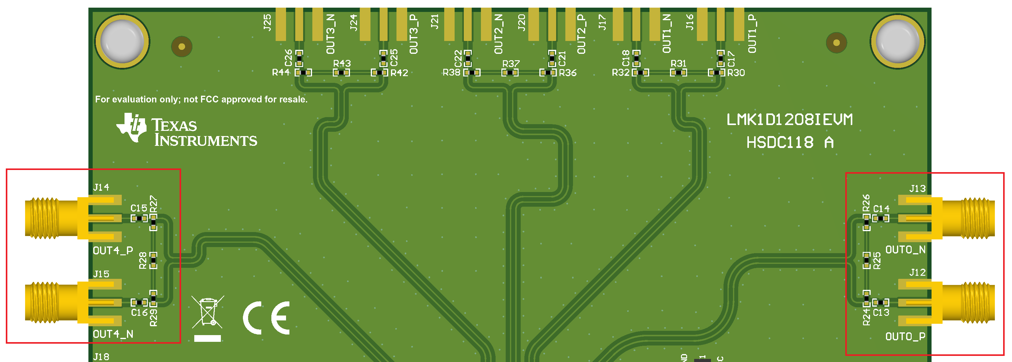
The LMK1D1208I generates up to 8 LVDS outputs. Two outputs (OUT0 and OUT4) are available by default on the EVM through the following populated SMAs: J12, J13 (OUT0_P, OUT0_N) and J14, J15 (OUT4_P, OUT4_N).
The LVDS outputs are AC-coupled to their respective SMAs. Each output pair has the 100-Ω termination on the board already populated.
 Figure 7-1 Output Clock EVM Layout .