SNAU282 September   2022


  1.   Abstract
  2.   Trademarks
  3. 1Evaluation Board Kit Contents
  4. 2Quick Start
    1. 2.1 Quick Start Description
      1. 2.1.1 Clock Outputs Page Description
      2. 2.1.2 TICS Pro Tips
  5. 3PLL Loop Filters and Loop Parameters
    1. 3.1 PLL1 Loop Filter
    2. 3.2 PLL2 Loop Filter
  6. 4Default TICS Pro Mode
  7. 5Using TICS Pro to Program the LMK04832-SEP
    1. 5.1 Start TICS Pro Application
    2. 5.2 Select Device
    3. 5.3 Program the Device
    4. 5.4 Restoring a Default Mode
    5. 5.5 Visual Confirmation of Frequency Lock
    6. 5.6 Enable Clock Outputs
  8. 6Evaluation Board Inputs and Outputs
  9. 7Recommended Test Equipment
  10. 8Schematics
  11. 9Bill of Materials
  12.   A USB2ANY Firmware Upgrade
  13.   B TICS Pro Usage
    1. 11.1  Communication Setup
    2. 11.2  User Controls
    3. 11.3  Raw Registers Page
    4. 11.4  Set Modes Page
    5. 11.5  Holdover Page
    6. 11.6  CLKinX Control Page
    7. 11.7  PLL1 and 2 Page
    8. 11.8  SYNC / SYSREF Page
    9. 11.9  Clock Outputs Page
    10. 11.10 Other Page
    11. 11.11 Burst Mode Page

Other Page

The Other page contains some registers to control the GPIO pins of the LMK04832. Each pin has two fields, the first is the _TYPE field which allows the input or output mode of the pin to be defined. The second is the _MUX field which, when set for output, controls what the pin will output.
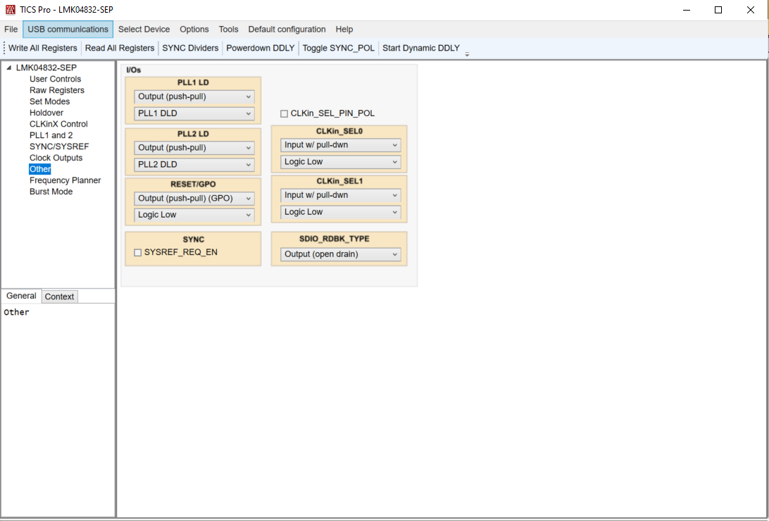
GUID-20220914-SS0I-DJR4-WVCR-M8JSX33WL70P-low.png Figure 11-10 TICS Pro - Other Page