SNLA382 March 2021 DS250DF230
2 QFN Pinout and Schematic Considerations
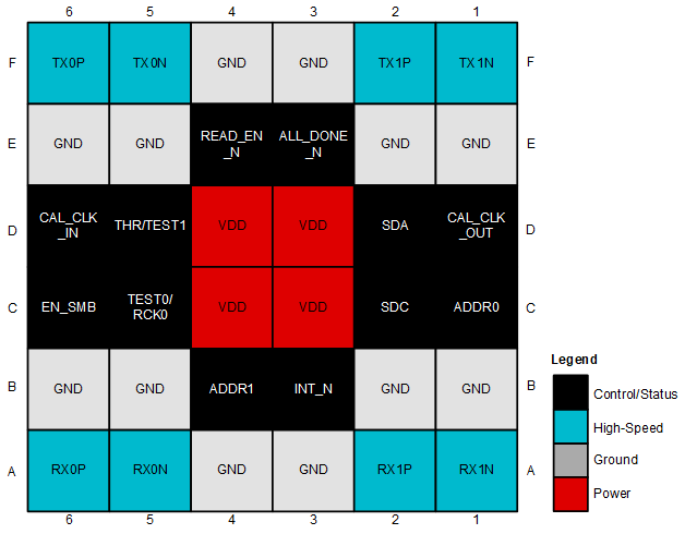
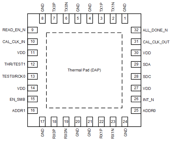
The following is a detailed comparison of differences between BGA and QFN packages.
 Figure 2-1 ZLS (BGA) 36-Package
Pinout
 Figure 2-2 RTV (QFN) 32-Package
Pinout
Figure 2-2 RTV (QFN) 32-Package
PinoutThere are no differences from a schematic and pinout standpoint in terms of the number or availability of the high-speed, control/status, and power pins. The only difference in pin count is the number of GND connections. There are 12 balls on the BGA package routed to GND. There are 8 pins and a large thermal pad on the QFN package that are internally routed to GND.