SNLA395 November 2021 DP83TD510E
1 Application Brief
Introduction
Power over Datalines (PoDL) for single-pair Ethernet (SPE) as it is explained in this document is standardized in the IEEE 802.3cg and IEEE 802.3bu. In 802.3bu, PoDL is specified for 100 and 1000 BASE-T1 Ethernet, 802.3cg adds support for 10 BASE-T1L.
Figure 1-1 shows a typical PoDL system consisting of power sourcing equipment (PSE) and a powered device (PD). The PSE is typically part of a switch, remote IO, PLC, or media converter. But it could also be a mid-span device without an Ethernet PHY. These all commonly consist of a PSE controller handling the power path and a coupling network combining power and data to one single twisted-pair line.
On the other side of this line, a PD like a sensor or an actuator is connected. Here a coupling network separates power and data. The power path is fed to a PD controller, responsible for handshaking and providing power to the next level of power tree. The data path is connected to an Ethernet PHY.
 Figure 1-1 PoDL System Simplified
The IEEE standards 802.3bu and 802.3cg describe how this works. The standards also specify power classes and types of devices to encode the data compatibility. The power classes are shown for reference in Table 1-1 and Table 1-2.
| 12-V Unregulated PSE | 12-V Regulated PSE | 24-V Unregulated PSE | 24-V Regulated PSE | 48-V Regulated PSE | ||||||
|---|---|---|---|---|---|---|---|---|---|---|
| Class | 0 | 1 | 2 | 3 | 4 | 5 | 6 | 7 | 8 | 9 |
| VPSE(max) (V) | 18 | 18 | 18 | 18 | 36 | 36 | 36 | 36 | 60 | 60 |
| VPSE_OC(min) (V) | 6 | 6 | 14.4 | 14.4 | 12 | 12 | 26 | 26 | 48 | 48 |
| VPSE(min) (V) | 5.6 | 5.77 | 14.4 | 14.4 | 11.7 | 11.7 | 26 | 26 | 48 | 48 |
| IPI(max) (mA) | 101 | 227 | 249 | 471 | 97 | 339 | 215 | 461 | 735 | 1360 |
| PClass(min) (W) | 0.566 | 1.31 | 3.59 | 6.79 | 1.14 | 3.97 | 5.59 | 12 | 35.3 | 65.3 |
| VPD(min) (V) | 4.94 | 4.41 | 12 | 10.6 | 10.3 | 8.86 | 23.3 | 21.7 | 40.8 | 36.7 |
| VPD(max) (W) | 0.5 | 1 | 3 | 5 | 1 | 3 | 5 | 10 | 30 | 50 |
| Class | 10 | 11 | 12 | 13 | 14 | 15 |
|---|---|---|---|---|---|---|
| VPSE(max) (V) | 30 | 30 | 30 | 58 | 58 | 58 |
| VPSE_OC(min) (V) | 20 | 20 | 20 | 50 | 50 | 50 |
| VPSE(min) (V) | 20 | 20 | 20 | 50 | 50 | 50 |
| IPI(max) (mA) | 92 | 240 | 632 | 231 | 600 | 1579 |
| PClass(min) (W) | 1.85 | 4.8 | 12.63 | 11.54 | 30 | 79 |
| VPD(min) (V) | 14 | 14 | 14 | 35 | 35 | 35 |
| VPD(max) (W) | 1.23 | 3.2 | 8.4 | 7.7 | 20 | 52 |
An understanding of how the complete procedure for implementing a PoDL system is important. The standard specifies (similar to standard Ethernet PoE) that a detection and classification phase is required. As the name implies, during detection the power sourcing equipment (PSE) senses if a compliant powered device (PD) is connected. If this is the case, it switches to the next stage, the classification. Now the PSE reads out from the PD what power classes are supported. If PSE and PD support the same classes, the PSE turns the power on.
Even though the steps are similar to standard Ethernet PoE, they are implemented in a different manner. For the detection, a PoE PSE must sense a resistor on the PD side. A PoDL PSE must sense a Zener diode on the PD. To do this, the PSE provides a constant current on the line and measures the voltage. The Zener diode limits this voltage and the PSE senses this as a valid detection if the voltage is in a certain range.
Also, the classification is implemented in a different way. Where PoE uses a constant voltage from the PSE and a current sink on the PD to signal the power class, PoDL implements a simple digital one-wire communication, the serial classification protocol (SCCP).
Both detection and classification in a PoDL system is not always required. A system can implement a fast start-up and skip the classification, so only the detection mechanism needs to be implemented and the system can save time at start-up. Also, it is possible to skip the detection, which makes the classification necessary. A system without detection and classification is not allowed according to the standard.
A proprietary system without any detection and classification is possible from the technical side, but the user must make sure to connect only equipment supporting this.
Maintain full voltage signature (MVFS): the PD must draw a current of more than 11 mA every 10 ms as long as the PSE should keep the line powered. If this does not happen, the PSE assumes the PD got disconnected and powers the link off. To distinguish between a low-power PD and a disconnected PD, the PD must draw more than 11 mA in pulses.
PSE Implementation
A PSE can be implemented using four states:
- Detection (Provide constant current, sense voltage on the line)
- Classification (Communicate with the PD)
- Power On
- Sleep
From these steps it is already possible to derive a simplified block diagram to visualize what is needed. Figure 1-2 shows how a PSE controller might look. There is a constant current source needed for detection, as well as for the classification. A window comparator monitors the voltage on the line and signals to the MCU if the voltage is in a valid range.
For the classification, the MCU senses the level on the line and can drive the line to low through a MOSFET. Together with the current source, this implements everything needed to do the SCCP.
The power switch not only gets the enable signal from the MCU, but also the current limit for the power class must be set accordingly and we need to have some feedback about the current.
A power switch is used to power on, as Figure 1-2 shows. This gets not only the enable signal from the MCU, but also the current limit for the power class must be set accordingly and we need to have some feedback about the current. The feedback is needed to detect if a device got disconnected. But also can be used for power management in a multi-port PSE and for monitoring.
The optional DC/DC is needed when implementing a PSE supporting multiple power classes with different voltage levels. It gets configured by the MCU to the needed output voltage before turning on the power switch.
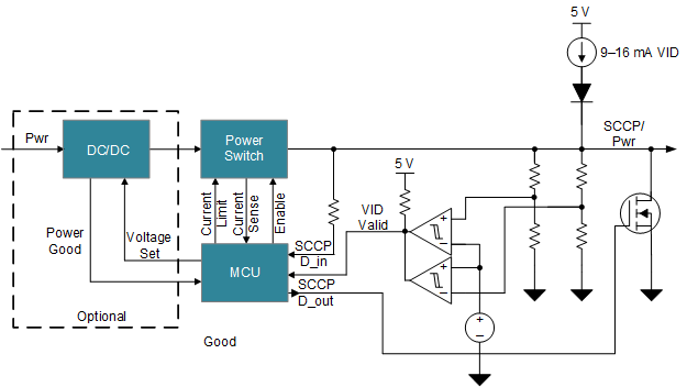 Figure 1-2 PoDL PSE Simplified
In addition to these mentioned steps an additional prebias is needed. This prebias will bias the connected PD to 3.15 V–3.575 V during sleep state and allow a transition to detection, when the current is between 1.25 and 1.85 mA. This allows to keep the PD working and allows a faster detection and finally turn on.
Detection
A systems starts in state one, with the detection. The standard gives the necessary details. The PSE must provide a constant current of 9 to 16 mA with an open loop voltage of 4.75 to 5.5 V. A PD should be recognized as valid, when the sense voltage is between 4.05 and 4.7 V and it should be rejected if the voltage is below 3.7 V or just 5 mV below the open loop voltage.
Figure 1-3 visualizes the limits. With an open loop voltage of 5 V, the red bars are the voltage ranges, where a PSE hast to reject a PD. The yellow bars show the voltage ranges, where it is OK to accept or reject. If the voltage is in the limits of the green bar, the PSE must accept the PD.
 Figure 1-3 Detection Voltages
Figure 1-4 shows how the detection can be implemented in hardware. This circuit consists of two blocks, the window comparator and the current source. The window comparator is build using a TLV6700, as this integrates two comparators and a reference, so just a few components are needed. The current source is build using a transistor Q5 and a resistor R5, this gives a current of roughly 12 mA but will drift over temperature. However the drift is low enough to stay in the 9- to 16-mA window.
 Figure 1-4 Detection Current Source
The current source can be disconnected using Q6. This implementation of current source has some drawbacks. The 5-V power supply rail must be able to sink enough current, so the rail will not be pulled up when the current source is disconnected or no device is connected. And when enabling the source, the slew rate is fast and can violate the specified current slew rate of 1 A/ms.
To overcome these problems, this current source can be extended by a small operational amplifier driving the base of Q5, as shown in Figure 1-5. Q1 is now used for enabling the current source. The resistor divider will set the current and together with C1 also the slew rate can be programmed. Besides the improved slew rate, also the current consumption is lower as it can be fully turned off. D1 is added to make sure not to violate the maximum open loop voltage of 5.5 V. This allows more tolerance on the 6.5 V rail.
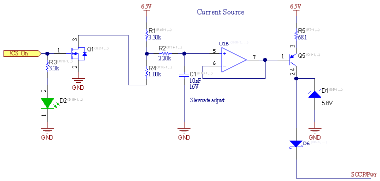 Figure 1-5 Improved Detection Current Source
Classification
After the detection has successfully completed, the classification can be implemented. As previously mentioned, classification is using a very low speed one-wire protocol. The basic structure looks as shown in Figure 1-6. The PSE integrates a current source and both PSE and PD can pull the line low. The PSE and PD also needs to sense the line.
 Figure 1-6 Classification Simplified
Every SCCP transaction as shown in Figure 1-7 starts with a falling edge, driven by the PSE. The length of time that the line is at low level defines if a logic one or zero is transmitted. The PD must measure this time. For the PD to send data, still the PSE will start with a falling edge and now the PD will pull the line low. Depending on when it releases the line, a logic one or zero is transmitted.
 Figure 1-7 SCCP Time Slots
The timings used here are rather slow, a time slot is specified to be between 2.7 and 3.3 ms. This slow timing makes it easy to be implemented in software on an MCU.
Figure 1-8 shows how the SCCP is implemented. The same current source from the detection is used as a pullup here. The line is driven low with a small FET (Q3), additionally a second FET (Q4) is used for preventing turn on of the communication FET, when the line is powered. To read what is happening on the line, it is simply current limited, clamped, and fed to the MCU.
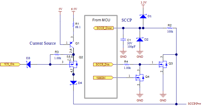 Figure 1-8 SCCP Implementation
On the software side, the PSE can implement SCCP with an SPI peripheral. This gives an easy way to offload the communication and the software does not need to take care of the timings, as they are controlled by the hardware. All that is needed is to prepare an array of data to be sent out. The received data can be later read out by going through the received data.
Power Switch
To turn on the power at the output and have an adjustable current limit, a TPS26601 is used as shown in Figure 1-9. The current limit can be adjusted by biasing the ILIM resistor R2. This allows to use one configuration for all supported power classes and adjusting the limit from the MCU.
The TPS2660 allows to measure the current, so the MCU has information about the current flow on each port.
 Figure 1-9 Power Switch
The MVFS requires to detect a current of 2.5–10 mA as threshold. A current that low cannot be seen using the TPS26601, so an additional low side current sense is added.
Figure 1-10 shows the circuit. The green block labeled PWR contains the eFuse circuit with the TPS26601. The current monitoring signal of the eFuse is used for bypassing a low side shunt using comparator U3 and FET Q2. When the eFuse measures a current of roughly more than 50 mA, the 4-Ω shunt resistor R7 gets shorted to keep the total internal resistance low and the power dissipation low. When a low current is drawn from the circuit, Q2 is not conducting and the current must pass R7. The voltage drop here can be measured with U2 and is used to sense if the MFVS criteria is fulfilled.
Both signals, from U2 and from U3 are diode ORed together and provided to the MCU to signal that either MVFS pulses are sensed or enough current is drawn.
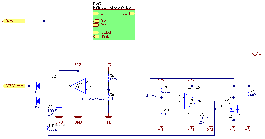 Figure 1-10 Current Sense MFVS
Sleep Mode and Prebias
During sleep state as well as idle state a VSleep Voltage must be applied at the output. The standard specifies this voltage to be in the range of 3.15 V - 3.575 V. This low voltage can power the PD controller and keep the circuit active to allow a fast reaction of the detection circuit and power the device up again.
To go back from sleep state to power on state, it is needed to go through detection and classification again.
When coming from idle state, the same voltage as in sleep state is applied, but to go over to detection, it is needed to have the prebias valid criteria fulfilled. The current during prebias is monitored and as soon as the current consumption is between 1.25 mA and 1.85 mA for at least 0.1 ms it is signaled as valid and detection can begin.
This mechanism brings a benefit to speed up the detection, as it will charge up all capacitors on the line and the PD controller can be running. So when the current source for detection is turned on, the voltage on the line can rise fast and the detection can be completed quickly.
Figure 1-11 shows how this part of the PSE is implemented. It consists of four blocks, voltage source, current sense, window comparator and an enable circuit. The voltage is derived from the 6.5-V supply and regulated to 3.5 V using U4A. This voltage is chosen over the anyhow existing 3.3-V rail, to have enough headroom for voltage drop caused by R14 and D5 and still meeting the specification.
The 3.5 V voltage is fed over R14 to a simple high side switch implemented using Q3 and Q4 and the diode D5. The voltage drop of R14 is monitored and amplified for the window comparator U6. This window comparator signals to the MCU when the measured current is in the valid range.
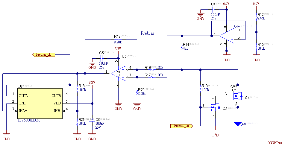 Figure 1-11 Prebias Circuit
These are all the necessary analog blocks to implement a PSE controller compliant to IEEE 802.3bu and 802.3cg. There are a couple of timings and slew rates that are different between the cg and bu standard that need to be considered in the software controlling all the state transitions. Also the different slew rates during power up require a different configuration of the eFuse TPS26601, which results in a different assembly variant. Important to mention, this example implementation is focused on 24 V classes only, so to extend this to other voltage levels some changes might be needed.
Coupling Network
Handling the power as described before is half of the system, the second half of this is combining the PSE controller with an Ethernet PHY. With standard Ethernet PoE as shown in Figure 1-12, power can be injected from the PSE either on the so called spare pairs (the unused twisted pairs on a network cable when using 10/100 Mbit/s Ethernet) or in the middle tap of the data transformer (when using 1 Gbit/s Ethernet or not having the additional pairs on the cable). There are always at least two pairs available, what makes it simple to carry power.
 Figure 1-12 Standard Ethernet PoE
When looking at a single pair Ethernet connection it gets a bit more difficult, as only one pair is available. So it is needed to use one conductor for plus and the other for minus. This also makes it necessary to add kind of a frequency filter into the lines. The power is almost a pure DC signal, except during classification where we have a frequency of 333 Hz. Whereas the data signal is always an AC signal with different frequency ranges, depending if using 10, 100 or 1000 BASE-T1.
For coupling power and data together there are basically two ways, as shown in Figure 1-13 and Figure 1-14. Using the capacitive coupling, AC signals can pass to the PHY through capacitors, but are isolated with an inductor from the power. This circuit can be implemented with a very small footprint for low isolation voltages. When a higher isolation voltage is required it gets larger and more expensive as the capacitors have to be rated for the desired voltage.
The inductive coupling uses a small transformer for the data coupling, a small cap on the right side to open the loop for DC and again an inductor for the power path. The capacitor here is not critical for the isolation, it just must withstand the operating voltage. The isolation voltage is defined by the voltage rating of the transformer.
Tests show, the inductive coupling is more robust to EFT noise than the capacitive approach.
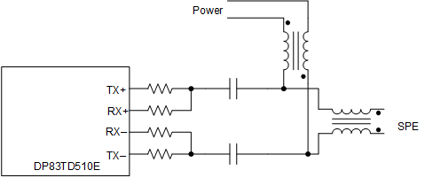 Figure 1-13 Capacitive Coupling
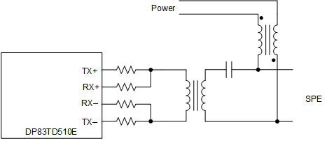 Figure 1-14 Inductive Coupling
This implementation has been tested with an inductive coupling using 10 BASE-T1 and power class 12. As transformer ICI70CGI-102N from TDK and 74930200 from Würth is tested and working fine. As DMI for filtering the power lines, PID150H-251M from TDK and 744870471 from Würth is used and as CMC a RCM70CGI-471N from TDK.
Test Results
The design is tested against the parameters given in the IEEE802.3cg standard when given there, otherwise against 802.3bu.
Detection Circuit
Figure 1-15 shows an example of the parameters for the detection as given by the standard. Item 1–4 are set with the current source itself, item 5 is defined by design and not measured. Item 6 is given by the combination of current source, window comparator and the software controlling this. Last item 7 is only given by the thresholds of the comparator.
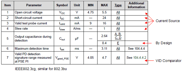 Figure 1-15 Tested Parameters Detection
Circuit
Figure 1-15 Tested Parameters Detection
CircuitThe results of the tests of items 1-3 and 7 are shown in Figure 1-16. All items are passed and within the limits.
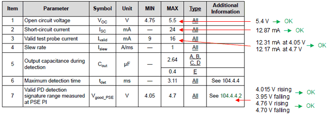 Figure 1-16 Tested Parameters Detection
Circuit - Results
Figure 1-16 Tested Parameters Detection
Circuit - ResultsFigure 1-17 shows the rise times and delays of the circuit. For this test, the output is loaded with a resistive load of 470 Ω. It can be seen, right after the current source is enabled, the output voltage and current starts to rise with a slope of 250 µs to 12 mA, which equals 50 mA/ms and is in the limits. This could also be made faster, but a faster current slew rate can cause together with the filter inductors a larger over- or undershoot.
The VID valid signal gets active for a short time during rise of the output current and voltage. However, this signal is further filtered in software and the valid signal must be held valid for at least 1 ms for a valid detection, so the 60-µs pulse is not causing problems.
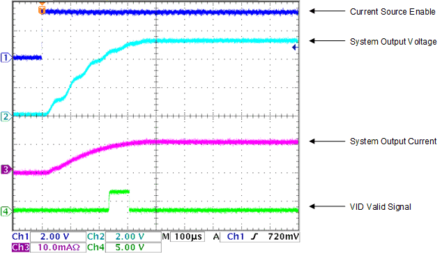 Figure 1-17 Detection Timing Rising Edge
The same timing is verified for the fall time of the current as well, see Figure 1-18. The fall time here is even a bit slower, so also in the limits.
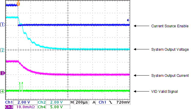 Figure 1-18 Detection Timing Falling
Edge
Figure 1-18 Detection Timing Falling
EdgeTurn on Behavior Without SCCP
The next thing to look at is the overall behavior from connecting a device until power up with SCCP disabled. Figure 1-19 shows what is going on during power up. This can be split into 3 phases. Phase 1 is where the prebias is active and the output is charged to approximately 3 V. After this is completed (when the current is between 1.25 and 1.85 mA), the detection circuit gets enabled, phase 2. The output current increases to 12 mA and the voltage on the line also increases to 4 V as limited by the connected PD. This signals a valid detection and in phase 3, the output gets turned on and the voltage rises 30 ms to the full output voltage.
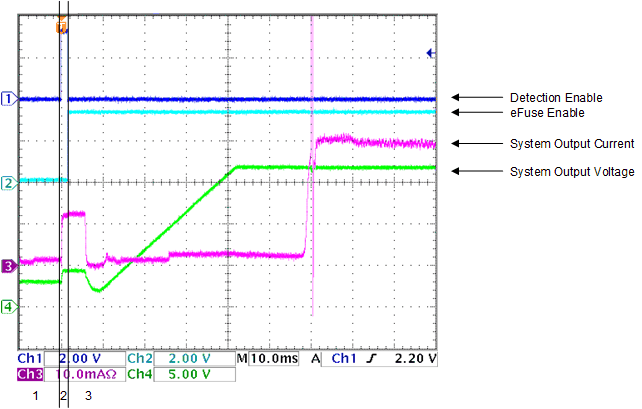 Figure 1-19 Detection and Power on
Things become more complicated when SCCP is enabled. Figure 1-20 explains what is going on.
- Port disabled, no prebias active
- Prebias and detection
- Prebias phase, port gets pre-charged to 3 V and as soon as current reaches the valid range, detection circuit gets enabled.
- Detection phase, current source gets turned on and the voltage rises into valid range.
- SCCP reset pulse, PSE drives line low for 10 ms to reset the PDs SCCP controller.
- SCCP presence detect, PD drives the line low after 0.5–1.5 ms for 2.5–7.5 ms. PSE detects this sequence and initiates SCCP transfer.
- SCCP communication, PSE sends out the broadcast address command (0xCC) to the PD followed by a scratchpad read command (0xAA). The PD answers with the class and type information, followed by a CRC8.
- After the PSE verified the information from the PD about the power class, supports a compatible class and the checksum is valid as it turns on the port.
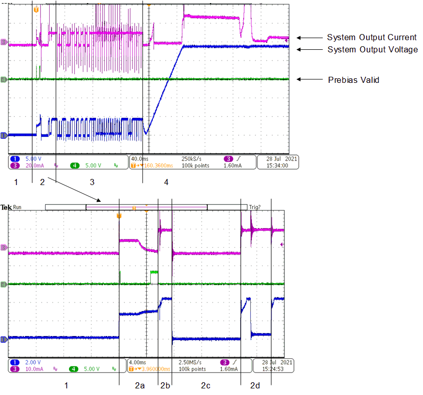 Figure 1-20 Detection and Power on With SCCP