SNLU313 August 2022 DP83TG720R-Q1 , DP83TG720S-Q1
3.1.1 Setup
- Create a new schematic and navigate to the Signal
Integrity – IBIS palette in the drop-down. Select the IO component and place two. This
example will demonstrate the RX_CLK to TX_CLK connection.
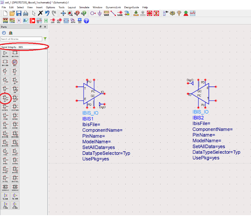
- Double click the IO component and select the dp83tg720r.ibs file for both components.
- This component functions as either the IBIS_O
(Output) buffer or the IBIS_I (Input) buffer depending on the enable state. When the
buffer is enabled, it functions as an IBIS_O (Output) buffer. When disabled, it behaves as
an IBIS_I (Input) buffer.
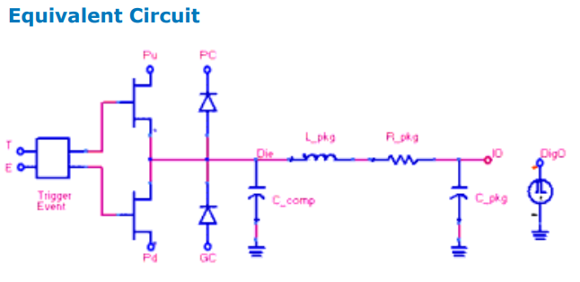
In the Input mode, the DigIO pin assumes the value 0 or 1 depending on the voltage at the IO pin compared to the model’s Vinl and Vinh parameters.
Further description of all the IBIS components available in ADS can be found here:
Next, wire each one of the pins starting with the enable pin.
Double click on the left component, and click on the Model tab. You will see this model is active-low. This means pulling this pin low will make this part an Output, while providing a voltage source greater than or equal to 1 V will make it an Input. An Active-High model would be the inverse.
To make the left IO an Output and the Right IO an Input, make the connections as follows. The DC source can be found in the Basic Components palette.
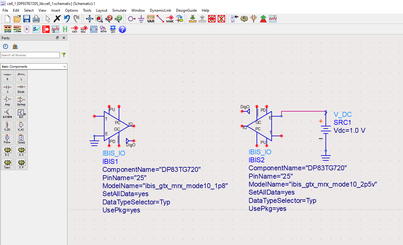
Make the rest of the connections as follows
Trigger Pin – For the Output component, this is the input to the buffer. Place a Pulse source from the Source-Time Domain palette, and configure it to [0,1.8] V and 125 Mhz. For the Input component, this pin is unused.
IO – Connecting these two pins together will form the channel. In between, add a transmission line of your choosing. Ideal T-Lines are found in the Tlines-Ideal Palette.
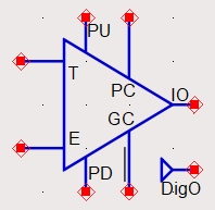
PU(Pullup), PC (Power clamp) – Connect these to the desired logic level of operation.
PD (Pulldown), GC (Ground clamp) - Connect to ground.
DigO – Digital output pin for the input device. Insert a pin name here to monitor this later.
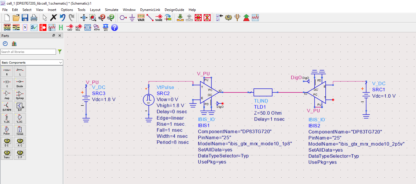
Now that the necessary connections are made, double click on the left IBIS component, and navigate to the Pin tab. Here, select the pin and available models. Select the RX_CLK pin and use the default Model. Click Apply.
Do the same on the right IBIS component, but select the TX_CLK pin.