SNOA987B March 2018 – October 2024 OPA2388-Q1 , OPA388 , THS4521 , TLV3201 , TLV7021
Design Goal
| Overcurrent Levels | Supply | Transient Response Time | ||
|---|---|---|---|---|
| IIN (min) | IIN (max) | V+ | V– | t |
| 0A | 1.0A | 5V | 0V | < 10µs |
Design Description
This high-speed, low-side overcurrent detection option is implemented with a single zero-drift fast-settling amplifier (OPA388) and one high-speed comparator (TLV3201). This circuit is designed for applications that monitor fast current signals and overcurrent events, such as current detection in motors and power supply units.
The OPA388 is selected for wide bandwidth with ultra-low offset and fast slew rate. The TLV3201 is selected for the fast response due to a small propagation delay of 40ns and rise time of 4.8ns. This allows the comparator to quickly respond and alert the system of an overcurrent event all within the transient response time requirement. The push-pull output stage also allows the comparator to directly interface with the logic levels of the microcontroller. The TLV3201 also has low power consumption with a quiescent current of 40µA.
Typically for low-side current detection, the amplifier across the sense resistor can be used in a noninverting configuration. The application circuit shown, however, uses the OPA388 as a differential amplifier across the sense resistor. This provides a true differential measurement across the shunt resistor and can be beneficial in cases where the supply ground and load ground are not necessarily the same.

Design Notes
- To minimize errors, choose precision resistors and set R1 = R3, and R2 = R4 .
- Select RSENSE to minimize the voltage drop across the resistor at the max current of 1A.
- Due to the ultra-low offset of the OPA388 (0.25µV), the effect of any offset error from the amplifier is minimal on the mV range measurement across RSENSE .
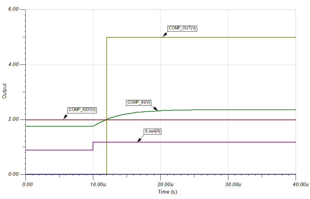
- Select the amplifier gain so COMP_IN reaches 2V when the system crosses its critical overcurrent value of 1A.
- Traditional bypass capacitors are omitted to simplify the application circuit.
Design Steps
- Determine the transfer equation
where R1 = R3 and R2 = R4.
- Select the SENSE resistor value
assuming a maximum voltage drop of 10mV with a load current of 1A to minimize
the voltage drop across the resistor.
- Select the amplifier gain such that
COMP_IN reaches 2V when the load current reaches the critical threshold of 1A.
Set:
- Calculate the transimpedance gain
of the amplifier to verify the following AC simulation results:
Design Simulations
COMP_IN Transimpedance AC Simulation Results

Transient Response Simulation Results
References
- Texas Instruments, Advantages of Using Nanopower, Zero Drift Amplifiers for Battery Voltage and Current Monitoring in Portable Applications, application note
- Texas Instruments, Current Sensing in No-Neutral Light Switches, technology brief
- Texas Instruments, GPIO Pins Power Signal Chain in Personal Electronics Running on Li-Ion Batteries, application brief
Design Featured Comparator
| TLV3201 | |
|---|---|
| VS | 2.7V to 5.5V |
| tPD | 40ns |
| Input VCM | Rail-to-rail |
| Vos | 1mV |
| Iq | 40µA |
| TLV3201 | |
Design Alternate Comparator
| TLV7021 | |
|---|---|
| VS | 1.6V to 5.5V |
| tPD | 260ns |
| Input VCM | Rail-to-rail |
| Vos | 0.5mV |
| Iq | 5µA |
| TLV7021 | |
Design Featured Op Amp
| OPA388 | |
|---|---|
| VS | 2.5V to 5.5V |
| Input VCM | Rail-to-rail |
| Vout | Rail-to-rail |
| Vos | 0.25µV |
| Vos Drift | .005µV/°C |
| Iq | 1.7mA/Ch |
| Ib | 30pA |
| UGBW | 10MHz |
| OPA388 | |
Design Alternate Op Amp
| THS4521 | |
|---|---|
| VS | 2.5V to 5.5V |
| Input VCM | Rail-to-rail |
| Vout | Rail-to-rail |
| Vos | 20µV |
| Vos Drift | µV/°C |
| Iq | 1mA/Ch |
| Ib | 0.6µA |
| UGBW | 145MHz |
| THS4521 | |