SNOA998 June 2018 TLV3201 , TLV7011
Design Goals
| Supply | Oscillator Frequency | |
|---|---|---|
| Vcc | Vee | f |
| 5 V | 0 V | 1 MHz |
Design Description
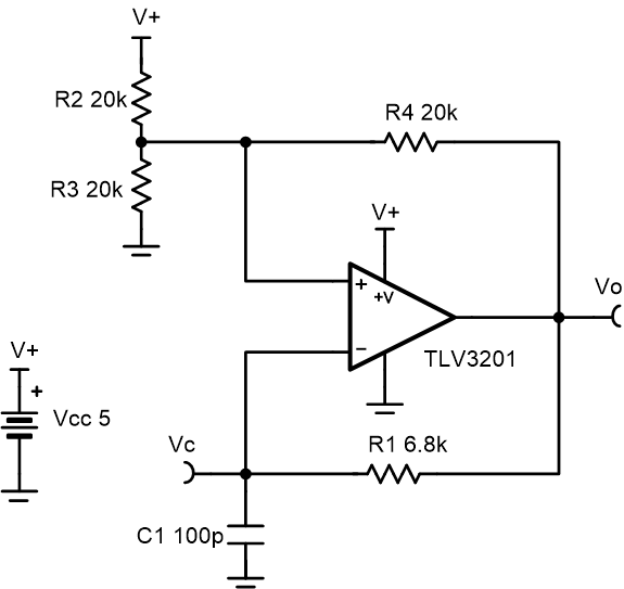
The oscillator circuit generates a square wave at a selected frequency. This is done by charging and discharging the capacitor, C1 through the resistor, R1. The oscillation frequency is determined by the RC time constant of R1 and C1, and the threshold levels set by the resistor network of R2, R3, and R4. The maximum frequency of the oscillator is limited by the toggle rate of the comparator and the capacitance load at the output. This oscillator circuit is commonly used as a time reference or a supervisor clock source.
Design Notes
- Comparator toggle rate and output capacitance are critical considerations when designing a high-speed oscillator.
- Select C1 to be large enough to minimize the errors caused by stray capacitance.
- If using a ceramic capacitor, select a COG or NPO type for best stability over temperature.
- Select lower value resistors for the R2, R3, R4 resistor network to minimize the effects of stray capacitance.
- R2, R3, and R4 can be adjusted in order to create a duty cycle other than 50%.
Design Steps
- When R2 = R3 = R4, the resistor network sets the oscillator trip points of the non-inverting input at one-third and two-thirds of the supply.
- When the output is high, the upper trip point will be set at two-thirds of the supply to bring the output back low.
- When the output is low, the lower trip point will be set at one-third of the supply in order to bring the output back high.
- The timing of the oscillation is controlled by the charging and discharging rate of the capacitor C1 through the resistor R1. This capacitor sets the voltage of the inverting input of the comparator. Calculate the time to discharge the capacitor.
- Calculate the time to charge the capacitor.
- The time for the capacitor to charge or discharge
is given by 0.69R1C1. With a target oscillator frequency
of 1 MHz, the time to charge or discharge should be 500 ns.
- Select C1 as 100 pF and R1 as 6.8 kΩ (the closest real world value).
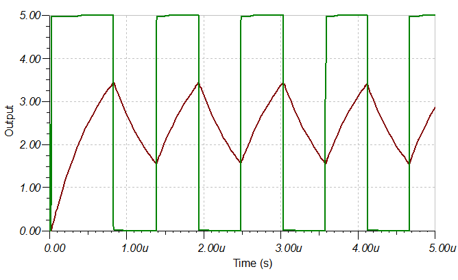
Design Simulations
Transient Simulation Results
Design References
See Analog Engineer's Circuit Cookbooks for TI's comprehensive circuit library.
See circuit spice simulation file, SBOMAO3.
For more information on many comparator topics including hysteresis, propagation delay and input common mode range please see, TI Precision Labs.
Design Featured Comparator
| TLV3201 | |
|---|---|
| Vss | 2.7 V to 5.5 V |
| VinCM | Rail-to-rail |
| tpd | 40 ns |
| Vos | 1 mV |
| VHYS | 1.2 mV |
| Iq | 40 µA |
| Output Type | Push-Pull |
| #Channels | 1 |
| TLV3201 | |
Design Alternate Comparator
| TLV7011 | |
|---|---|
| Vss | 1.6 V to 5.5 V |
| VinCM | Rail-to-rail |
| tpd | 260 ns |
| Vos | 0.5 V |
| VHYS | 4 mV |
| Iq | 5 µA |
| Output Type | Push-Pull |
| #Channels | 1 |
| TLV7011 | |