SNVSAO6C September 2017 – March 2018 LMZM33603
PRODUCTION DATA.
- 1 Features
- 2 Applications
- 3 Description
- 4 Revision History
- 5 Pin Configuration and Functions
- 6 Specifications
-
7 Detailed Description
- 7.1 Overview
- 7.2 Functional Block Diagram
- 7.3
Feature Description
- 7.3.1 Adjusting the Output Voltage
- 7.3.2 Feed-Forward Capacitor, CFF
- 7.3.3 Output Current vs Output Voltage
- 7.3.4 Voltage Dropout
- 7.3.5 Switching Frequency (RT)
- 7.3.6 Synchronization (SYNC)
- 7.3.7 Input Capacitors
- 7.3.8 Output Capacitors
- 7.3.9 Output On/Off Enable (EN)
- 7.3.10 Programmable Undervoltage Lockout (UVLO)
- 7.3.11 Power Good (PGOOD)
- 7.3.12 Overcurrent Protection (OCP)
- 7.3.13 Thermal Shutdown
- 7.4 Device Functional Modes
- 8 Application and Implementation
- 9 Power Supply Recommendations
- 10Layout
- 11Device and Documentation Support
- 12Mechanical, Packaging, and Orderable Information
3 Description
The LMZM33603 power module is an easy-to-use integrated power solution that combines a 3-A, step-down, DC/DC converter with power MOSFETs, a shielded inductor, and passives into a low-profile package. This power solution requires as few as four external components and eliminates the loop compensation and magnetics part selection from the design process.
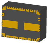
The 9 mm × 7 mm × 4 mm 18-pin, QFN package is easy to solder onto a printed circuit board and allows a compact, low-profile, point-of-load design. The full feature set, including power good, programmable UVLO, prebias start-up, and overcurrent and over-temperature protection, make the LMZM33603 an excellent device for powering a wide range of applications.
Device Information
| DEVICE NUMBER | PACKAGE | BODY SIZE (NOM) |
|---|---|---|
| LMZM33603 | QFN (18) | 9.00 mm × 7.00 mm |
space
space
space

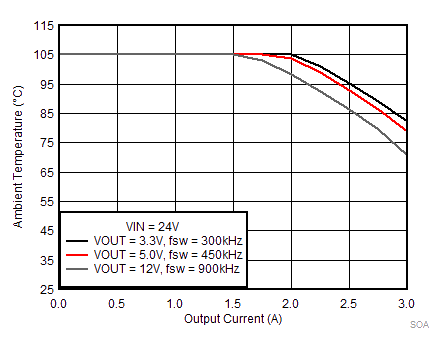
Safe Operating Area
