SNVSCU7A July 2025 – August 2026 LM65440-Q1 , LM65460-Q1
PRODMIX
- 1
- 1 Features
- 2 Applications
- 3 Description
- 4 Device Comparison Table
- 5 Pin Configuration and Functions
- 6 Specifications
-
7 Detailed Description
- 7.1 Overview
- 7.2 Functional Block Diagram
- 7.3
Feature Descriptions
- 7.3.1 Output Voltage Selection
- 7.3.2 EN Pin and Use as VIN UVLO
- 7.3.3 Mode Selection
- 7.3.4 Adjustable Switching Frequency
- 7.3.5 Dual Phase Operation
- 7.3.6 Dual Randrom Spread Spectrum (DRSS)
- 7.3.7 Internal LDO, VCC UVLO, and BIAS Input
- 7.3.8 Bootstrap Voltage (BST Pin)
- 7.3.9 Soft Start and Recovery From Dropout
- 7.3.10 Safety Features
- 7.4 Device Functional Modes
-
8 Application and Implementation
- 8.1 Application Information
- 8.2
Typical Application
- 8.2.1 Design Requirements
- 8.2.2
Detailed Design Procedure
- 8.2.2.1 Custom Design With WEBENCH® Tools
- 8.2.2.2 Choosing the Switching Frequency
- 8.2.2.3 FB for Adjustable or Fixed Output Voltage Mode
- 8.2.2.4 Inductor Selection
- 8.2.2.5 Output Capacitor Selection
- 8.2.2.6 Input Capacitor Selection
- 8.2.2.7 CBOOT
- 8.2.2.8 External UVLO
- 8.2.2.9 Maximum Ambient Temperature
- 8.2.3 Application Curves
- 8.3 Best Design Practices
- 8.4 Power Supply Recommendations
- 8.5 Layout
- 9 Device and Documentation Support
- 10Revision History
- 11Mechanical, Packaging, and Orderable Information
8.2.3 Application Curves
The applications curves are measured using the LM65460EVM. Unless otherwise specified the following condition apply: TA = 25ºC, VIN = 12V.

| VOUT = 5V | Auto Mode | L = 3.3μH |

| VOUT = 5V | Auto Mode | L = 2.2μH |

| VOUT = 5V | Auto Mode |
| VOUT = 5V | Auto Mode | L = 2.2μH |

| VOUT = 5V | Auto Mode |

| VOUT = 5V | Auto Mode |

| VOUT = 5V | 2.1Mhz | L = 0.68μH | LM65480 |

| VOUT = 5V | 2.1MHz | L = 0.68μH | LM65480 |

| VOUT = 5V | Auto Mode | L = 0.68μH | LM65480 |

| VOUT = 3.3V | 2.1Mhz | L = 0.68μH | LM65480 |

| VOUT = 3.3V | 2.1Mhz | L = 0.68μH | LM65480 |

| VOUT = 3.3V | Auto Mode | L = 0.68μH | LM65480 |

| VOUT = 3.3V | VIN = 12V | IOUT = 8A |

| VOUT = 3.3V | VIN = 12V | IOUT = 6A |
| No EMI Filter | LM65460EVM |

| VOUT = 3.3V | VIN = 12V | IOUT = 8A |

| VOUT = 3.3V | VIN = 12V | IOUT = 6A |
| With EMI Filter | LM65460EVM |

| IOUT = 6A | VIN = 12V | VOUT = 5V |

| IOUT = 0A to 6A (1A/μs) | VIN = 12V | FPWM Mode | VOUT = 5V |

| IOUT = 50mA | VIN = 12V | VOUT = 5V |

| IOUT = 0A to 6A (1A/μs) | VIN = 12V | Auto Mode | VOUT = 5V |

| IOUT = 50mA | VIN = 12V | Auto Mode | VOUT = 5V |

| IOUT = Short Circuit | VIN = 12V | VOUT = 5V |
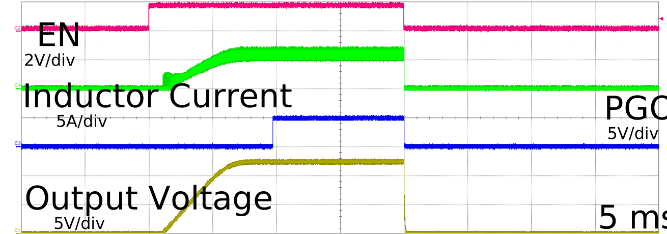
| IOUT = 6A | VIN = 12V | Auto Mode | VOUT = 5V |

| IOUT = 6A | 2100kHz | VIN = 12V | VOUT = 5V |
| LM65460EVM |
Table 8-3 Typical System Specifications
| PARAMETER | TEST CONDITIONS | MIN | TYP | MAX | UNITS | |
|---|---|---|---|---|---|---|
| Isupply | Input supply current | Vin = 12V, Vout = 5V, Iout = 0A, LM65460-Q1, 2.1MHz | 8.7 | µA | ||
| Vin = 24V, Vout = 5V, Iout = 0A, LM65460-Q1, 2.1MHz | 5.6 | µA | ||||
| Output ripple | Vout = 5V | Vin = 12V, Iout = 6A, FPWM | 11.8 | mVpp | ||
| Vout = 5V | Vin = 12V, Iout = 0A, AUTO | 23.8 | mVpp | |||
| Vout = 3.3V | Vin = 12V, Iout = 6A, FPWM | 10.7 | mVpp | |||
| Vout = 3.3V | Vin = 12V, Iout = 0A, AUTO | 17 | mVpp | |||
| η | Peak efficiency | Vin = 12V, Vout = 5V, Iout = 4A , LM65460-Q1, 2.1MHz | 94 | % | ||
| Vin = 12V, Vout = 5V, Iout = 3A , LM65460-Q1, 400kHz | 96.5 | % | ||||
| Vin = 12V, Vout = 3.3V, Iout = 4A , LM65460-Q1, 2.1MHz | 92 | % | ||||
| Vin = 12V, Vout = 3.3V, Iout = 3A, LM65460-Q1, 400kHz | 95.6 | % | ||||
| Loop response | Crossover frequency | Vin= = 12V, Vout = 3.3V, Cout = 22µF + 10µF, L = 0.68uH | 220 | kHz | ||
| Gain margin | Vin= = 12V, Vout = 3.3V, Cout = 22µF + 10µF, L = 0.68uH | –18 | dB | |||
| Phase margin | Vin= = 12V, Vout = 3.3V, Cout = 22µF + 10µF, L = 0.68uH | 51 | ° | |||
| Load transient | 10% to 90% load transient output voltage ripple | Vin = 12V, Vout = 5V, 2.1MHz, AUTO, 10% to 90% load | 368 | mVpp | ||
| Vin = 12V, Vout = 5V, 2.1MHz, FPWM, 10% to 90% load | 338 | mVpp | ||||
| Vin = 12V, Vout = 3.3V, 2.1MHz, AUTO, 10% to 90% load | 212 | mVpp | ||||
| Vin = 12V, Vout = 3.3V, 2.1MHz, FPWM, 10% to 90% load | 214 | mVpp | ||||