SNVU191B October 2012 – December 2021 LMR12020
8 PCB Layout
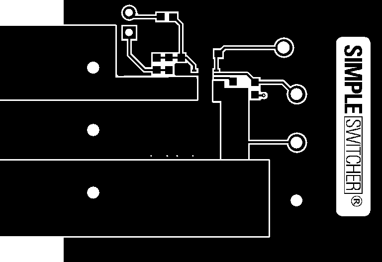 Figure 8-1 Top Copper
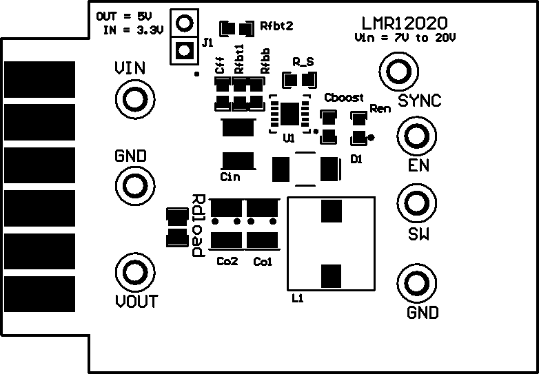 Figure 8-2 Top Overlay
 Figure 8-3 Internal Layer 1
 Figure 8-4 Internal Layer 2
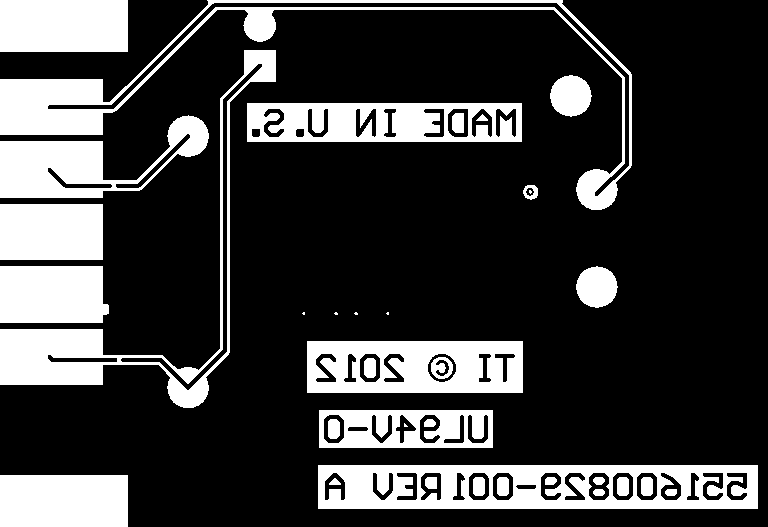 Figure 8-5 Bottom Copper
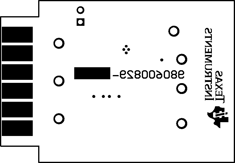 Figure 8-6 Bottom Overlay
SNVU191B October 2012 – December 2021 LMR12020
 Figure 8-1 Top Copper
 Figure 8-2 Top Overlay
 Figure 8-3 Internal Layer 1
 Figure 8-4 Internal Layer 2
 Figure 8-5 Bottom Copper
 Figure 8-6 Bottom Overlay