SNVU735 September 2020 LV14360
3 Board Layout
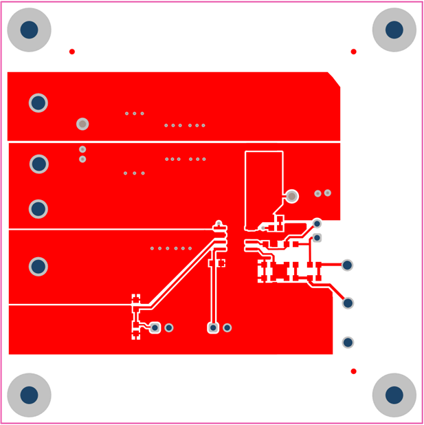
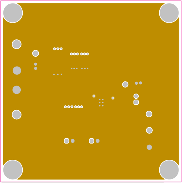
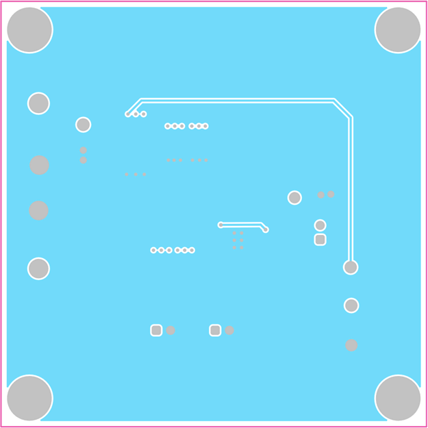
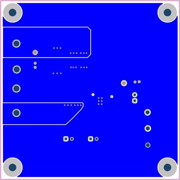
Figure 3-1 to Figure 3-4 show the board layout for the LV14360PEVM. The PCB consists of a 4-layer design. 2-oz copper planes are applied on all four layers to dissipate heat with an array of thermal vias under the thermal pad to connect to all four layers.
 Figure 3-1 Top
Layer
 Figure 3-2 Middle
Layer 1
 Figure 3-3 Middle
Layer 2
 Figure 3-4 Bottom
Layer