SNVU838A October 2022 – November 2022 LMR51450
5 Board Layout
Figure 5-1 through Figure 5-6 show the board layout for the LMR51450 EVM. The EVM offers resistors, capacitors, and test points to configure the following:
- Output voltage
- Precision enable
- Set frequency
The 12-pin WSON package offers a very small solution size. The PCB consists of a 4-layer design. There are 2-oz copper planes on the top and bottom and 1-oz copper mid-layer planes to dissipate heat with an array of thermal vias to connect to all four layers.
Test points have been provided for ease of use to connect the power supply and required load, and to monitor critical signals.
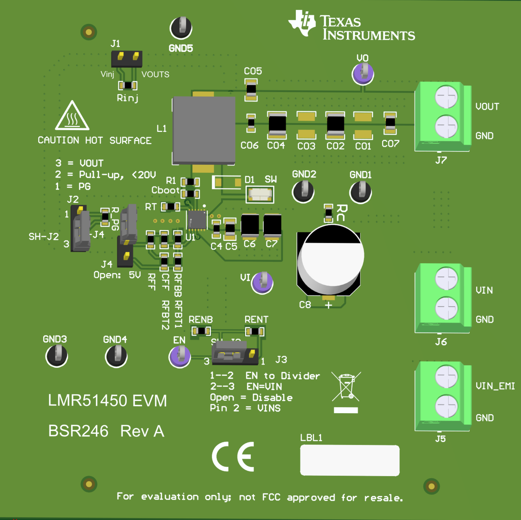 Figure 5-1 Top
3D View
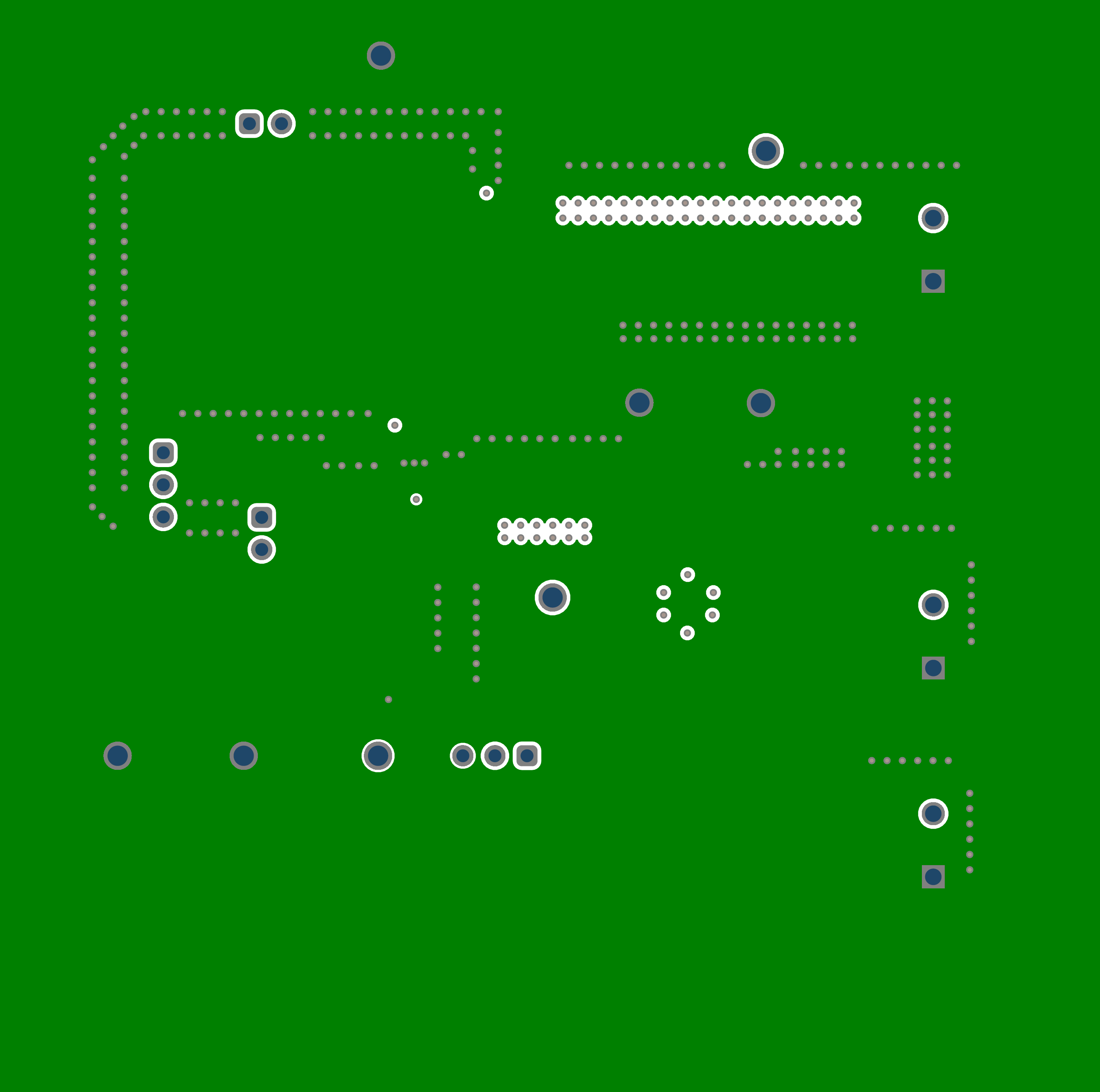 Figure 5-3 Signal Layer 1 - Ground Plane
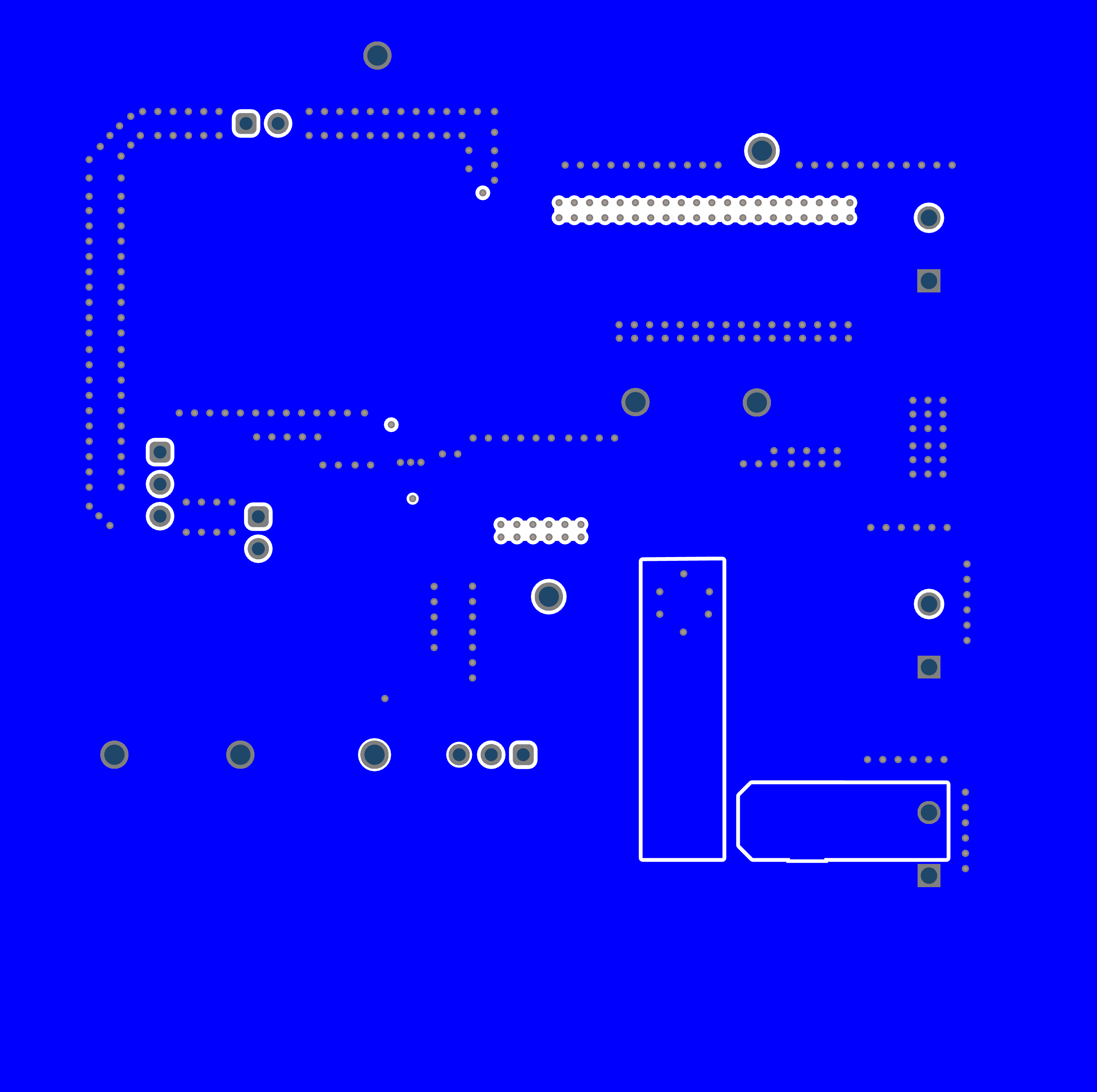 Figure 5-5 Bottom Layer
 Figure 5-2 Top
Layer
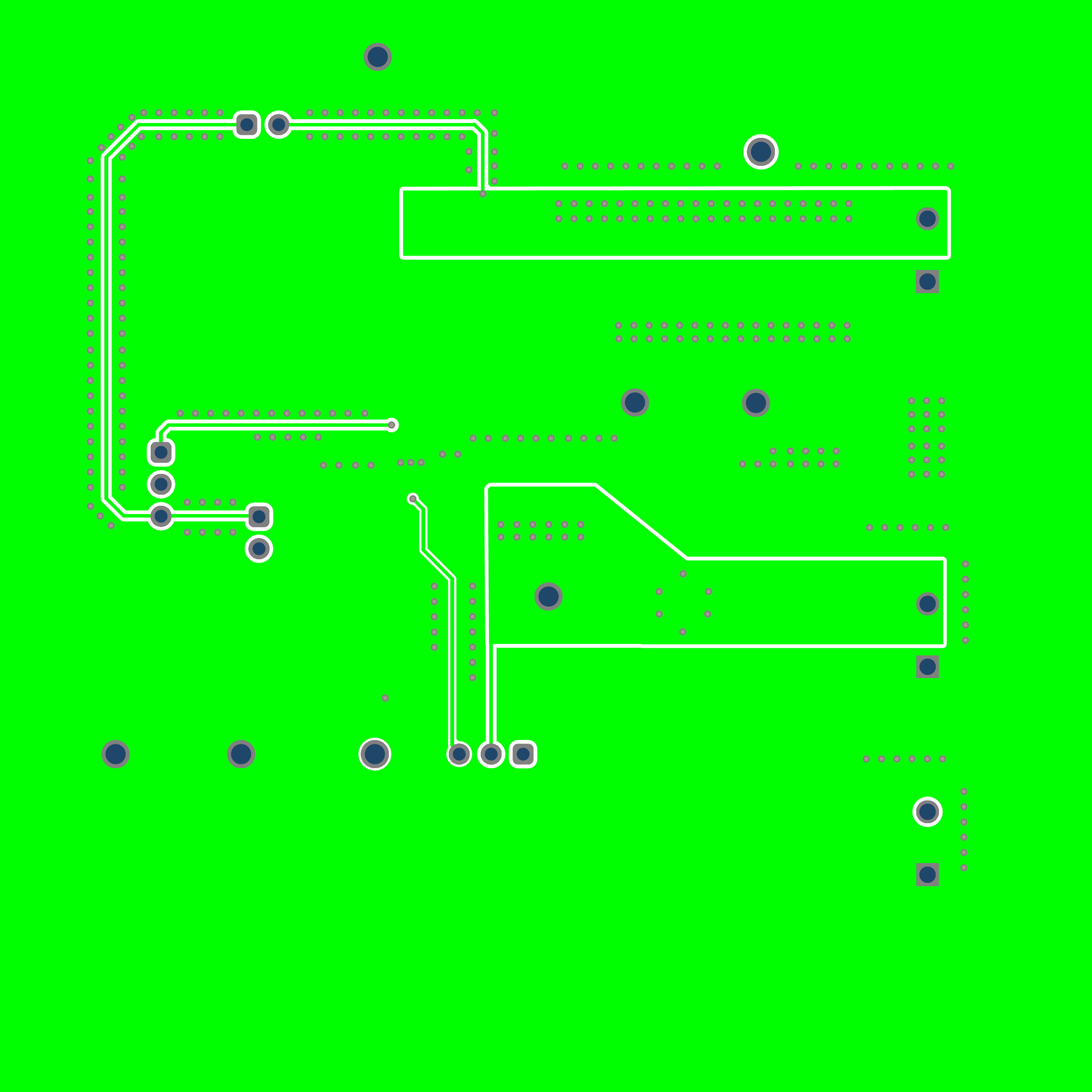 Figure 5-4 Signal Layer 2 - Routing
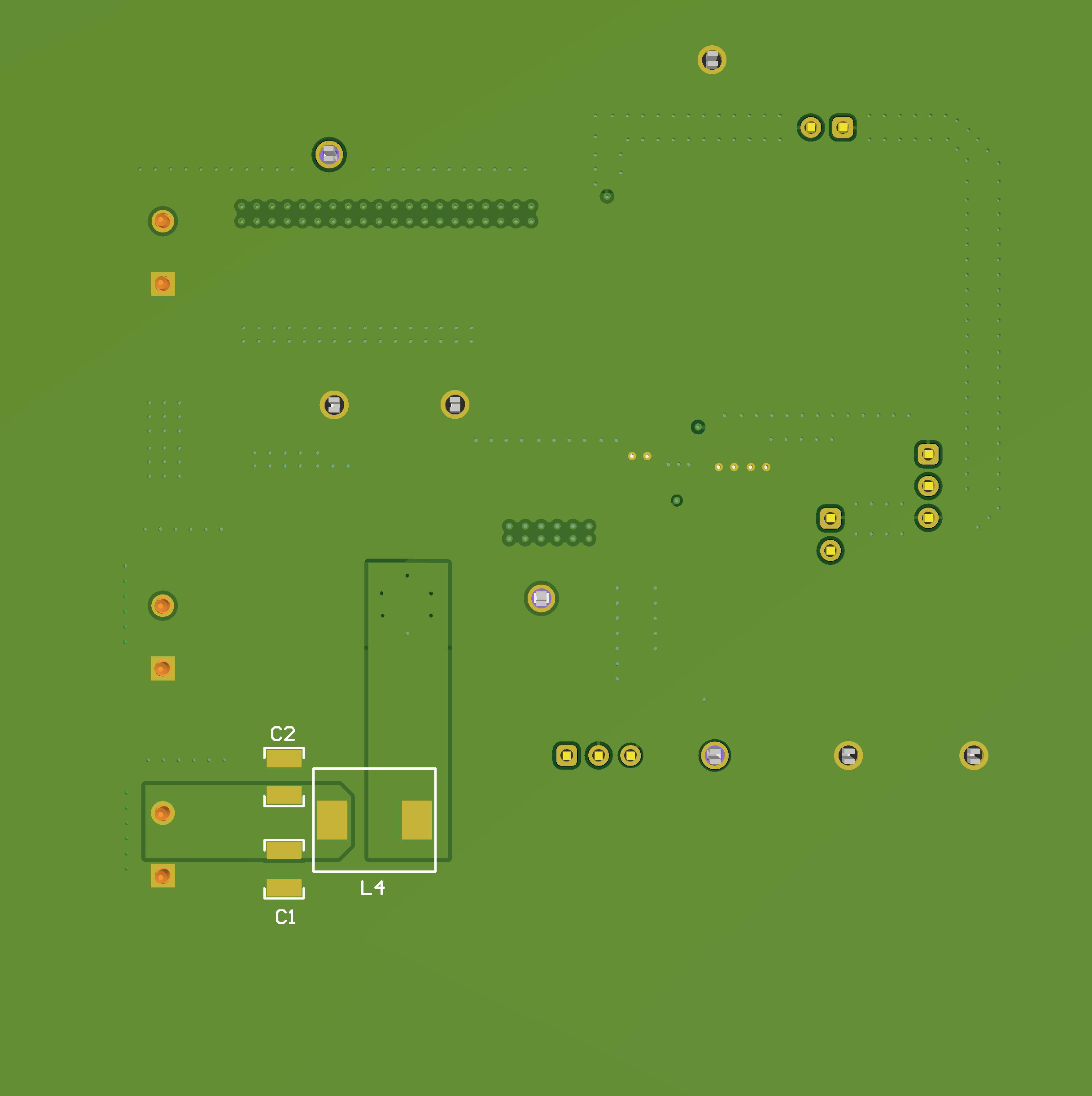 Figure 5-6 Bottom 3D view