SSZT132 September 2021 OPA391 , OPA392
In applications measuring high current levels through a resistive shunt, the differential voltage developed across a tiny shunt is typically very small in order to minimize the power dissipation inside the sensing resistor – in the range of just a few millivolts. Contrary to popular belief, the slew rate of the op amp has little bearing on its performance due to the small signal nature of these measurements. Instead, the operational amplifier (op amp)’s gain bandwidth (GBW) is most critical parameter.
This is the first article in a four-part series discussing how to increase system accuracy and efficiency with op amps built on TI’s new, proprietary complementary metal-oxide semiconductor (CMOS) precision process technology. This CMOS process technology has pushed the limits of GBW vs. quiescent current (IQ) to unprecedented levels, helping the high-precision OPA391 op amp attain a GBW of 1 MHz on mere 24 µA of IQ.
In this article, I’ll discuss a detailed implementation of high current, high speed, low-side current shunt applications using the ultra-low IQ OPA391 and its higher-speed counterpart, the OPA392, to show the impact of its higher bandwidth.
Figure 1 (left) shows an improper connection of TI’s OPA391 for a low-side high-current application resulting in a measurement error caused by inclusion of R_trace parasitic resistance as part of the shunt resistor. In order to eliminate the error, you must connect the sensing input resistor, R3, at the bottom of the resistive shunt, Rshunt – see Figure 1 (right). Low ohmic shunt resistors sometimes include four terminals to aid in this connection.
 and proper connection for low-side high current measurement (right)") Figure 1 Improper connection for low-side high current measurement (left) and proper connection for low-side high current measurement (right)
Figure 1 Improper connection for low-side high current measurement (left) and proper connection for low-side high current measurement (right)It is natural to assume that in high-speed monitoring circuits with large output-voltage signals, the slew rate of the amplifier would be the limiting factor in terms of response time. But this rationale fails to consider the fact that in order for the amplifier to slew, you must apply a large input signal (1 V or higher) at the input terminals. Since in order to minimize the power dissipation inside the shunt, high current monitoring circuits use a tiny shunt resistor, the resulting input voltage is very small, in the range of millivolts, which will not force the amplifier to slew. Instead, the response time of the circuit will be controlled by the small-signal rise time of the amplifier defined in Figure 1:
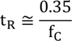
where fC = GBW/GCL is the effective bandwidth of the amplifier for a given close-loop gain, GCL.
Figure 2 shows the OPA391 monitoring a 10-A Ishunt current across a 400-µΩ shunt resistor with a gain of 1,001 V/V. You would expect that the OPA391, with a slew rate of 1 V/µs, would take just 4 µs for the output to reach 4 V. It is clear from the simulation below, however, that it takes much longer for the OPA391 output to respond because as you may recall the response time of the circuit is a function of the OPA391’s gain-bandwidth product, GBW, and close-loop gain, GCL, of the application and not its slew rate. This results in a rise time, tR, of 350 µs – almost 100 times longer than you may have at first expected.
 Figure 2 Rise time of the OPA391 low-side current shunt signal for G = 1,001
How can you speed up the op amp’s response time in high-speed, high-current monitoring applications? Obviously, one way to improve the response time is to decrease the gain of the circuit. Since the small-signal rise time of the amplifier output signal is a function of gain, lowering the close-loop gain from 1,001 V/V down to 101 V/V should shorten the rise time tenfold, from 350 µs down to 35 µs. And that is exactly what happens – see Figure 3.
 Figure 3 Rise time of the OPA391 low-side current shunt signal for G = 101
In order to decrease the response time further while maintaining the same output voltage range, it would take one-order-of-magnitude lower gain and a 10 times larger shunt resistor – 4 mΩ instead of 400 µΩ. As expected, placing the OPA391 in a gain of 10 V/V lowers the rise time down to 3.5 µs, and at this point, the slew rate of the OPA391’s finally dominates the settling time of the op amp, as illustrated in Figure 4. However, increasing Vshunt to 400 mV increases the power dissipation inside the shunt resistor to 40 W (P = 100 A × 400 mV), which may not be acceptable.
 Figure 4 Rise time of the OPA391 low-side current shunt signal for G = 10
So let’s ask again – if there anything else you can do to speed up the response time while maintaining the output voltage range, without increasing the power dissipation inside the shunt resistor? You could cascade two OPA391 amplifiers (see the application note, “Cascading Precision Op Amp Stages for Optimal AC and DC Performance”), each with a gain of 10 and a 400-µΩ shunt, but this solution is expensive and takes up board space. Or you can use the new OPA392 – because of its much higher gain bandwidth of 13 MHz, you may obtain a faster response time in gain of 101 V/V than OPA391 was able to get in gain of 10 V/V (Figure 5). But, just like everything in nature comes at a cost, this faster settling time comes at the price of OPA392 higher quiescent current of 1.2mA.
 Figure 5 Rise time of the OPA392 low-side current shunt signal for G = 101
You can employ a number of techniques, used alone or in combination, to optimize high-speed low-side current shunt measurements. But the exact details of the application requirements like various trade-offs of gain, size of shunt resistor, quiescent current and topology used, must be carefully considered in terms of their effect on circuit response time, power efficiency and total cost before the optimal solution may be achieved that meets your performance needs. The new OPA391 and OPA392 make your job a bit easier.
In the next installment of this series, we’ll discuss how to achieve accurate gain error and drift with a switched-gain transimpedance amplifier.
Additional resources
- Catch up on other installments in this technical article series.