SSZT335 february 2020 DAC43401 , DAC53401 , LM34936 , LM5176
As I discussed in the first installment of this series, one option to control output voltage (VOUT) for USB Type-C Power Delivery (PD) and wireless charging applications is to use switching resistors. This article will explain a different approach that requires fewer components and signal lines called modulated voltage programming.
Modulated voltage programming
You may recall from part 1 that switching resistors require three switched resistor branches and three control signals to produce the four voltages needed for USB Type-C PD applications. Each switched resistor branch also requires a resistor-capacitor (RC) delay to control the speed of switching, in order to prevent falsely triggering the overvoltage protection (OVP) function of the four-switch buck-boost controllers. The actual hardware requires many additional components, and the solution can appear cumbersome and may not easily fit into compact designs. In such cases, you may need a different approach to reduce the number of components.
Figure 1 shows an example in which a modulated voltage source (VC) alters the feedback (FB) pin voltage. Therefore, Equation 1 determines the VOUT:
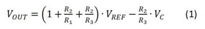
where VREF is the controller error amplifier reference voltage. Decreasing or increasing VC will adjust VOUT up or down, respectively.
There are two ways to control the VC level with a microprocessor. The first is to use an integrated digital-to-analog converter (DAC), and the second is to directly use the pulse-width modulation (PWM) signal produced by the microprocessor.
 Figure 1 Adjusting VOUT with a modulated voltage source
Controlling voltage through a DAC
USB Type-C PD and wireless charger systems usually have a microprocessor with an internal DAC. If it does not have an internal DAC, an external one like TI’s DAC43401 or DAC53401 can be used. As shown in Figure 2, the DAC can produce the required VC to adjust VOUT by programming the microprocessor to follow Equation 1.
False VOUT OVP can be a problem if the slew rate of VC is too quick. Therefore, when using microprocessor to control VC, make sure that the VC transition time is longer than the buck-boost DC/DC stage loop response time but does not exceed the applicable USB Type-C specifications.
 Figure 2 Using a DAC to control the VC
Controlling voltage through a PWM signal
The second approach is to use a General-Purpose Inputs/Output port (GPIO) of the microprocessor to produce a PWM signal. This PWM signal can be filtered out by an RC filter to produce a DC voltage before being fed into the FB pin, as shown in Figure 3. Changing the PWM duty cycle can dynamically adjust VOUT.
 Figure 3 Adjusting VOUT
through the PWM signal
Figure 3 Adjusting VOUT
through the PWM signalThe PWM filter will, however, introduce ripple voltages. If the low-pass corner frequency of the RC filter is much lower than the frequency of the PWM signal, both R3 and the FB pin will see an almost pure DC voltage. Therefore, the PWM will not cause significant ripples on the VOUT rail. I recommend choosing R4 and C1 such that the RC filter’s corner frequency is set to at least two decades below the frequency of the PWM signal, such that the ripple voltage at FB pin can be attenuated by at least 40 dB. Consequently, the selection of R4 and C1 should satisfy Equation 2:
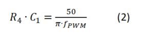
where fPWM is the frequency of the PWM signal.
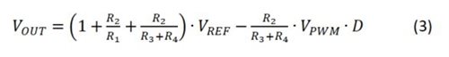
Assuming that the PWM signal’s duty cycle is D, the valley voltage is 0 V and the peak voltage is VPWM, then VOUT will satisfy Equation 3:
Using two-stage RC filters to avoid excessive delays
As mentioned above, the RC filter needs to attenuate the PWM by at least 40 dB. If the PWM signal frequency is limited, say to 200 kHz, the RC filter’s corner frequency will have to be set at 2 kHz, implying an RC filter time constant of about 80 ms. Since the settle time of an RC filter takes four times the time constant, the response to a step duty-cycle change will take more than 320 ms to settle, much longer than the USB Type-C PD specification of the voltage transition time. A solution is to use a two-stage RC filter, as shown in Figure 4.
 Figure 4 A two-stage RC filter to
reduce the delay time
Figure 4 A two-stage RC filter to
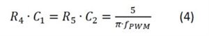
reduce the delay timeA two-stage RC filter provides 40 dB of attenuation per decade. In the same example, where the PWM signal is at 200 kHz, the filter’s corner frequency can be raised to 20 kHz, reducing the filter’s time constant to only 8 ms. The response to a step change of duty cycle will settle down within just 32 ms, which is fast enough to meet the USB PD applications. In general, choose the RC filter according to Equation 4:
Now, VOUT and the PWM duty cycle (D) satisfy Equation 5:
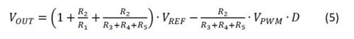
Note that VOUT will increase when D decreases. Programming the microprocessor according to Equation 5 will produce a PWM signal with the correct duty cycle to regulate the four-switch buck-boost output to the desired voltage level appropriate for a USB Type-C PD application.
Conclusion
For every technique showcased in this series, it is important to remember that false OVP events are possible if the switching between voltage levels is too quick. So make sure that the transition time is sufficient enough to satisfy the application and not trigger a false OVP event.
Additional resources
- See TI’s USB Type-C PD reference designs.
- Check out the LM34936 and LM5176 controller data sheets.
- Read Adjusting VOUT in USB Type-C™ and wireless charging applications, part 1.