SSZT555 January 2019 LMZM23600 , LMZM23601 , LMZM33602 , LMZM33603
In a previous post, “Enhancing DAQ performance for grid protection, control and monitoring equipment using DC/DC power modules,” we discussed how power modules offer lower electromagnetic interference (EMI) and output ripple, thus improving overall data acquisition (DAQ) performance. In this post, my colleague Sreenivasa and I will cover some of the other ways that power modules help improve DAQ performance compared to discrete power solutions.
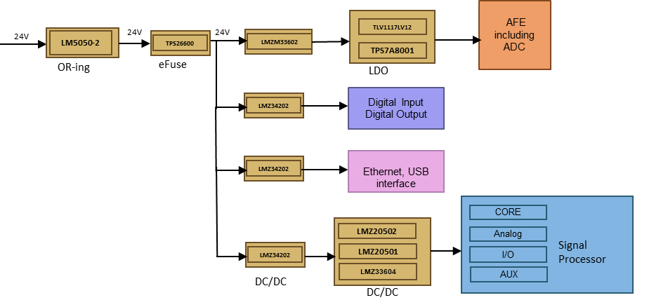
Power Architecture for a DAQ
 Figure 1 A DAQ Power Architecture Using Power Modules
Using power modules helps improve overall performance, efficiency and reliability. Power modules also provide these advantages:
- Output current in the same package provides design flexibility and scalability with optimized cost.
- A provision to improve light load efficiency with auto pulse frequency modulation (PFM) mode.
- Excellent transient response during load regulation.
- A compact solution through integration, innovative packaging and assembly.
- Improved power-module performance from careful passive component selection.
- Operation over a wide temperature range.
| Moving from conventional to intelligent substations | |

|
Learn more about intelligent substations by reading our new white paper, "Moving from conventional to intelligent substations." |
Improved Power-module Performance from Passive Component Selection
During the HTS test, inductors are placed close to the DC/DC converter, limiting airflow. The coating and/or binders of the iron powder begin to break down over time and in high-temperature conditions, which causes increased core loss and reduces power-supply efficiency. The problem is most evident at higher input voltages and higher switching frequencies. Figure 2 compares the efficiency degradation for an inductor over multiple input voltages before and after the HTS stress test.
Upon inspection, the inductor doesn’t normally look visibly damaged. The L and DCR values of the inductor may not change. However, exposure to high temperatures increases the AC impedance, as shown in Figure 2.
 Figure 2 Efficiency Degradation before and after HTS Testing and AC Impedance Change of the Inductor
Meanwhile, TI’s power modules integrate inductors that have excellent performance over time and with temperature increases. Figure 3 shows HTS test results for various inductors after exposure to high temperatures. Our power modules use inductors with minimal or no change in Q and core resistance after HTS tests.
 Figure 3 TI Power Modules Inductor HTS Performance
Also, our power modules undergo testing for working voltages to ensure that there is no insulation breakdown.
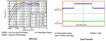
Efficiency (Overall and Light Load) with Auto PFM and Load Transient Response
This mode of operation results in excellent conversion efficiency at very light loads. When using auto-PFM mode, the output voltage at no load is approximately 1% higher than forced pulse width modulation (FPWM) operation. Figure 4 shows the efficiency graph for PFM and FPWM modes.
Load transient response is a measure of how well a supply copes with sudden changes in current demand or how well the supply follows changes in the load impedance. Load transient response is an increasingly important performance parameter, especially for a microprocessor or a field-programmable gate array that is characterized by a low core voltage, high current draw and fast load switching. Figure 4 shows the load transient response for a power module.
 Figure 4 Power-module Efficiency and Load Transient Response
You can improve transient response by adjusting the output capacitance, provided that you maintain sufficiently low equivalent series resistance. Adding input capacitance can enhance response for longer and/or deeper transient steps. Adding converter phases also improves transient response by increasing the effective switching frequency and by allowing smaller output inductors and capacitors, owing to the reduction in current per phase.
Reduced Solution Size
Our MicroSiP™ or QFN packaging technology can be used for rails requiring lower power. This packaging technology uses the bare DC/DC regulator die and embeds it in a thin printed circuit board substrate. Instead of using bond wires, the copper traces connect the die to the substrate, also shown in Figure 5. Examples include TI’s LMZM23601 and LMZM23600, which have the input bypass capacitor and inductor integrated in order to provide improved EMI performance.
 Figure 5 Power module packages
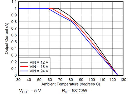
Operation over a Wide Temperature Range
 Figure 6 Ambient Temperature vs. Output Current
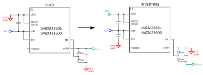
Generating an Inverted Supply Using Power Modules
 Figure 7 Converting from Buck to Inverted Buck Boost