SSZT568 december 2018 LMZM23600 , LMZM23601 , LMZM33602 , LMZM33603
Other Parts Discussed in Post: LMZM33603
(Note: Akshay Mehta co-authored this blog post.)
In my previous blog posts on improving data acquisition (DAQ) performance for grid protection, control and monitoring equipment, I discussed the need for interfacing multiple analog-to-digital converters (ADCs) and showed how you can improve DAQ performance and measurement accuracy by using the programmable real-time unit-industrial communication subsystem (PRU-ICSS) from a single Sitara™ processor, as well as using multiple high-performance, synchronizable sigma-delta ADCs.
| Moving from conventional to intelligent substations | |

|
Learn more about intelligent substations by reading our new white paper, "Moving from conventional to intelligent substations." |
In this post, my colleague Akshay and I focus on enhancing DAQ performance by using power modules for the generation of multiple voltage supplies, including 5-V, 3.3-V, 2.5-V and 1.8-V supply rails.
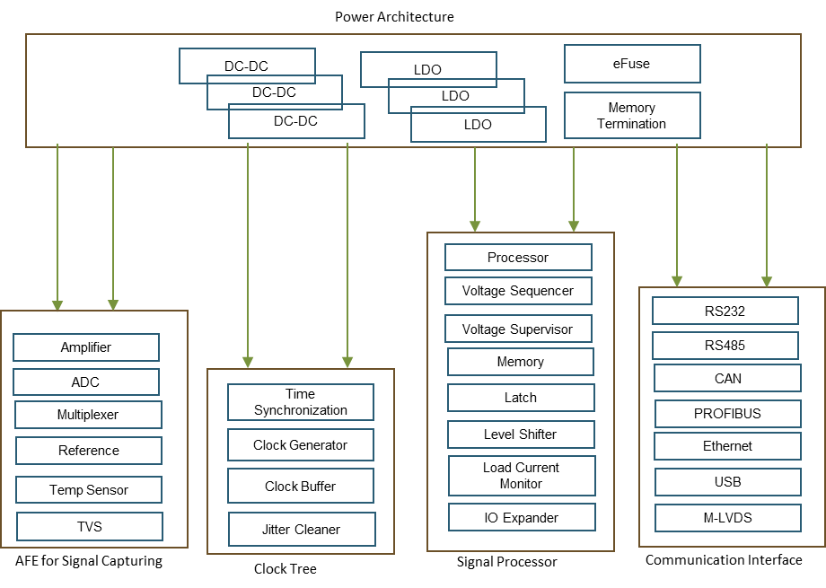
Figure 1 shows a DAQ with commonly configured subsystems, along with the devices or integrated circuits (ICs) found/used in them. Each subsystem has different voltage levels and load current requirements. The power architecture for a DAQ consists of multiple DC/DC converters, low-dropout regulators (LDOs), double-data-rate termination regulators, sequencers and monitors to generate and monitor various supply rails, and an eFuse for protection against input overload conditions.
 Figure 1 DAQ Subsystems, Including
Power Architecture
Figure 1 DAQ Subsystems, Including
Power ArchitectureDAQ Power Architecture Design Approaches
The choice of the appropriate power-supply architecture depends on the DAQ performance requirements, including efficiency, printed circuit board space, tight output regulation, load transient response and cost. You could derive the required supply rails from the backplane voltage using various combinations of DC/DC converters and LDOs.
A discrete power-supply implementation calls for power-supply design expertise. A discrete power-supply implementation uses an external inductor, switch and other external components. The DC/DC converter will occupy more board space, has poor efficiency and thermal performance. Discrete power supplies are also prone to failures, given a lack of protection against misuse (overloaded outputs, excessive input voltages) and shortened lifetimes due to component failures. An alternative approach for implementing DAQ power architecture is to use integrated power modules.
Advantages of Using a TI Power Module
A DC/DC buck-type power module integrates a synchronous switching regulator, inductor, field-effect transistors (FETs), compensation and other passive components into a single package. Through careful selection of onboard components, including an inductor, power modules perform with minimum variations over a wide voltage input and temperature range. Integrating the components within the power modules simplifies the design process, minimizes the footprint, increases reliability and shortens the design/qualification process enabling faster time to market.
Power modules are becoming more popular because of their fully characterized electrical/thermal performance. They can operate over a wide range of switching frequencies, enabling the use of smaller components, and can have a component footprint of <15 mm2 with a height of <2.0 mm. A non-isolated power module is compact, highly efficient and can deliver a high load current.
The Impact of Power Modules on DAQ Performance
Using a power module has multiple benefits, but two that impact DAQ performance the most are lower electromagnetic interference (EMI) and reduced output ripple. It is common for power designers to go through multiple board revisions to achieve EMI requirements and output ripple performance. Package selection and layout optimization are other important considerations to mitigate EMI and ensure a lower output ripple.
EMI
Meeting EMI requirements with sufficient margins according to Comité International Spécial des Perturbations Radioélectriques (CISPR) 11 or CISPR 22 is important for certification of any end-equipment. To mitigate EMI, power modules implement various techniques for critical loop-area optimization, thereby creating a smaller rate of current change (di/dt) loop area. Using shielded inductors further reduces EMI.
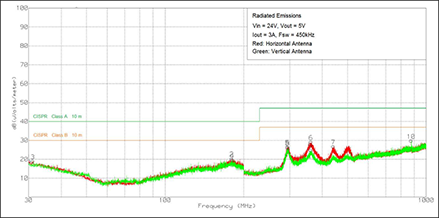
Figure 2 shows the radiated emission plot for TI’s LMZM33603 power module with a 3-A load, which is below CISPR Class A and B levels, making it easy to meet test requirements during certification.
 Figure 2 Radiated Emission for the LMZM33603 (5 v Output, 3 a Load)
To understand how power modules optimize the critical loop area, let’s take a look at component placement and package selection.
A buck converter generates a pulsating ripple current with high di/dt at the input. Without input capacitors, ripple current is supplied by the upper power source and the circulating ripple current results in increased conducted and radiated EMI.
Synchronous switching DC/DC regulators have both FETs integrated inside the package, which makes it easier to optimize the area of the critical path. With the two FETs integrated, only the input capacitor, CIN, requires proper placement. The input capacitor minimizes input voltage ripple, suppresses input voltage spikes and provides a stable system rail for the device, ensuring lower EMI. The ease of CIN placement depends on the packaging technology and pin-out. It is important to have the VIN and PGND pins close to each other. In TI power modules, we recommended placing the capacitor CIN closest to VIN and PGND, as shown in Figure 3, to minimize the area of the critical path. A small, low-value capacitor Ci is placed internal to TI power modules. In addition to CIN capacitor selection and optimizing critical path layout, the choice of power module packages discussed below also helps improve performance.
- Quad flat no-lead (QFN) packages have no external leads. The lack of lead lengths enables closer placement of the CIN to the VIN and PGND pins, thereby reducing the area of the critical path even further. QFN IC packages internally have the die pads bonded out to the pins through thin copper or gold wires, which adds parasitic inductance.
- To further reduce the area of the critical path, our HotRod™ technology eliminates the bond wires completely. The die is flipped so that its active side is facing down, and copper bumps are deposited on the die pads and soldered directly to the lead frame. Using copper bumps instead of bond wires lowers the series resistance, shrinking package size further and bringing the CIN even closer to the VIN and PGND pins. Figure 3 shows the QFN and HotRod™ packages.
 Figure 3 A.QFN Package Capacitor Placement, B.QFN Wire-bond and C. HotRod™ Packaging
Output Ripple
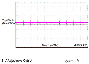
The output stage of the synchronous buck DC/DC converter plays an important role in meeting the target ripple current, output ripple voltage and output voltage overshoot requirements. The output ripple of a power module depends on the component selection, the layout and the load. In our power modules, selection of an inductor with low stray capacitance combined with an optimized layout (tightly laid out) ensures that minimal ripple from the switching pin gets coupled to the output pin VOUT, reducing ripple on the DC voltage output. Figure 4 shows the ripple from the power module and is <5-mV, which enables connection to sensitive analog circuits without performance variation.
 Figure 4 Power Module Output Ripple
Conclusion
TI’s power modules have multiple advantages simplifying the system design including:
- Minimal external components.
- Small size and high power density.
- Lower radiated EMI.
- Cooler operating temperatures.
- Higher efficiency and output accuracy.
- Faster load-transient response.
- Low output ripple.
- Improved load and input regulation.
Using internal inductors reduces magnetics selection efforts as well as enhances performance by shielding radiated emissions. Additionally, power modules incorporate extensive, well-thought-out protection mechanisms and are subject to more rigorous testing (more tests are done than what a typical end user would plan and test). While this post focused on advantages tied to improving DAQ performance, in another blog post, Akshay will look at other benefits of using power modules.
Additional Resources
- Check out the DC/DC power module portfolio.
- Read the white paper, “Simplify low EMI design with power modules.”