SSZT606 october 2018 LMZM33606
Oct 17, 2018
There are multiple applications, particularly in the test and measurement sector, where you need an external source or digital-to-analog converter (DAC) to program the output voltage of an inverting buck-boost regulator. To do that on a regular buck topology is fairly straightforward: all you have to do is inject current into the feedback node, using a voltage source with a series resistor, a current source or even a DAC, as shown in Figure 1.
 Figure 1 Programmable voltage with a
buck topology.
Figure 1 Programmable voltage with a
buck topology.But when you have to change the voltage of a regulator operating in the buck-boost topology, things start to get a little tricky.
You can configure a buck regulator in the buck-boost topology simply by reversing the ground and VOUT potentials and having the reference of the integrated circuit (IC) now be at the -VOUT potential. This means that the ground pin of the regulator IC is at -VOUT. The FB pin of the regulator is sitting over the -VOUT potential and not the ground potential, and this makes injecting current into the FB pin a tad difficult. To inject current into the FB pin in an inverting buck-boost topology, you’ll need to level-shift the signal from the voltage source/DAC. So in this article, I’ll show you a few different approaches how.
Let’s use the LMZM33606 from Texas Instruments as an example throughout. The LMZM33606 is a buck power module rated for 36V at the input and can supply a max load of 6A. Figure 2 shows how to set up the LMZM33606 as an inverting buck-boost regulator.
 Figure 2 Inverting buck-boost with the
LMZM33606.
Figure 2 Inverting buck-boost with the
LMZM33606.Approach No. 1: Level Shifter with a Single PNP
Using the LMZM33606 in these buck-boost applications, it’s possible to demonstrate a programmable output voltage range of -15V to -5V. With the current-source approach, you can reduce the output of the regulator in absolute magnitude. This means that you can set the feedback divider resistors such that the default output of the design is -15V. When adding an external current source, you can then program the output of the regulator to -5V. For the default of -15V, calculate the upper and lower feedback values as:
- RFBT = 100kΩ.
- RFBB = 7.42kΩ.
The simplest way to level shift a ground-referenced signal to inject current into the FB pin is to use a single p-channel n-channel p-channel (PNP)-type bipolar junction transistor (BJT). Figure 3 shows how a single PNP can be used as a level shifter.
 Figure 3 Implementation using a single
PNP.
Figure 3 Implementation using a single
PNP.The PNP Q1 has its base grounded and the emitter connects to the DAC/voltage source through a resistor. When the voltage source level increases above the base to emitter voltage (VBE) drop of the PNP, there will be current flow governed by Equation 1:
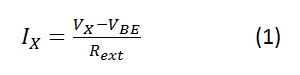
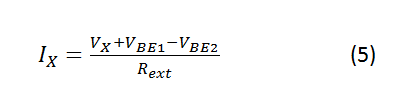
Rext is set at 50kΩ. Applying Kirchhoff’s current law at the FB node, you can calculate this current IX with Equation 2:
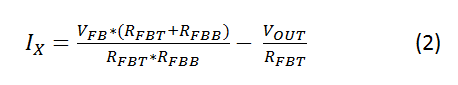
By substituting equation 1 in equation 2, we obtain equation 3 which finds the value of the programming voltage VX required to change the output voltage, VOUT:
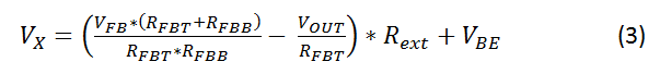
Turning Equation 3 around to Equation 4 gives you the VOUT that you can program based on the value of VX:
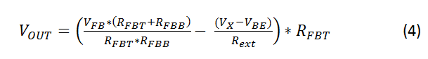
Equation 4 denotes the dependence of VOUT on the VBE of the transistor. The VBE of the transistor is itself dependent on the collector current, which when changed with temperature will result in some inaccuracies in the programmed VOUT.
The next approach shows how to remove VBE from the equation. Figure 4 shows a circuit with two PNP transistors that are connected such that the effect of VBE can be nullified.
Approach No. 2: Level Shifter with Two PNPs
 Figure 4 Implementation with two PNPs
to nullify VBE.
Figure 4 Implementation with two PNPs
to nullify VBE.This approach requires an additional PNP – ideally you should use two co-packaged PNP BJTs to ensure good matching between the two transistors. This approach will reduce errors in the programming of the output voltage.
The Q1 transistor has its base connected to the programming voltage source. The emitter then connects to another positive rail through a series resistor RS and the collector is grounded. This creates a voltage of VX + VBE at the emitter of the transistor. The Q2 transistor’s emitter connects to Q1’s emitter through resistor RX. RX sets the current to be injected into the FB node. With the base grounded, there is a +VBE generated at the emitter node of Q2. Equation 5 calculates the current flowing into the emitter (ideally) as:
From earlier, you know that the VBE of the transistor will depend on the collector current, expressed as Equation 6:
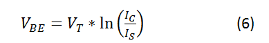
where IC is the collector current, IS is the saturation current and VT is the thermal voltage.
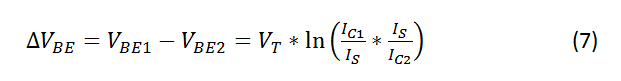
If the collector currents of the two transistors are very different, then the VBEs do not completely cancel each other out. Equation 7 expresses the difference in the two VBEs of the transistors as:
Simplified to Equation 8:
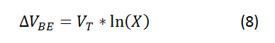
where X is the ratio of the two collector currents.
As you can see, if the two collector currents are equal, the VBEs will cancel out completely. In the configuration shown in Figure 4, it will be important to size the value of RS such that the difference in the collector currents is not considerable. For this example, I chose an RS of 10kΩ and an RX of 50kΩ. The delta in VBE will also change with the change in VT, which happens with changes in temperature.
Approach No. 3: a Modified Wilson Current Mirror
A good way to match collector currents is to use a current mirror. But there is one option better than a regular current mirror, and that is the Wilson current mirror. Figure 5 shows the schematic used for the Wilson current mirror.
 Figure 5 Implementation using a Wilson
Current Mirror.
Figure 5 Implementation using a Wilson
Current Mirror.In this approach, there is an additional BJT with its base connected to the collector of Q1. The emitter of Q3 connects to the VBE junction of the mirror. The programmed current flows through the collector of the Q3 transistor into the FB pin.
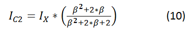
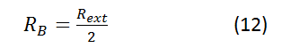
Ignoring resistor RB for now, Equation 9 calculates the reference current being injected in this setup as:
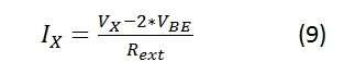
Equation 10 derives the ratio of injected current to reference current in this setup as:
Given the betas () of the transistors in high values, you can see that the Wilson current mirror gives you a lot more accuracy than the standard current mirror.
The Wilson current mirror doesn’t completely eliminate the dependence on VBE. But there is a pretty simple trick to get around this. Connecting a resistor RB from the source VX to the base of the mirror, as shown in Figure 5, creates a current flow that gets added to reference current IX. Rewriting Equation 9as Equation 11:
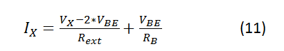
Equation 12 chooses RB such that:
Then Equation 13 is:
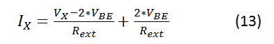
The VBE component in Equation 13 cancels out completely, resulting in Equation 14:
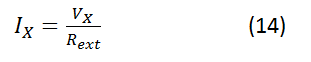
Equation 14 shows that the current injected into the FB node is based just on the programming voltage and has no dependencies on VBE.
Using any of these approaches can help generate a programmable output voltage for an inverting rail with just a few extra components. The circuit complexity will vary based on the system requirements. For applications that require very high fidelity, the Wilson current mirror is the best solution, as it gets the closest response to the programming voltage.
References
Toumazou, C., F.J. Lidgey and D.G. Haigh (Ed.), “Analogue IC Design: The Current-Mode Approach,” London: Peter Peregrinus Ltd., 1990.