SSZT662 July 2018 LDC2114
In the food industry, it is important to be able to clean and disinfect machinery to reduce the amount of bacteria and germs. These machines must have a user interface that can withstand the water and chemicals used for cleaning.
But building water and dustproof casings can be expensive and difficult, especially with a user interface that has buttons. Special waterproof buttons simplify the interface but result in a rather large, expensive and not customizable design. It is possible to create the buttons on a field transmitter in several different ways, which I’ll discuss in this post.
A waterproof and dustproof mechanical solution built around small push button would be a small and customizable solution, but there are complex mechanics and high production costs.
Regardless of the material the housing is made of, the product’s casing will deform as soon as it is touched. It may only be a few micrometers, but it’s enough to be sensed. The solution I’ll discuss in this text requires a casing made of conductive material, but even a thin conductive coating is sufficient for inductive buttons.
Measuring the Case Deformation
Many physical measurements can be reduced to either a capacitance or inductance change. It is possible to build a plate capacitor out of the casing metal and an electrode (such as one on a printed circuit board [PCB]) and detect the capacitance change. The capacitance will depend on the electrode size and distance. The change of the capacitance depends on the bending of the material.
Figure 1 shows how to build such a button. Milling one of the outer layers before pressing the layers together makes it possible to integrate such buttons in the PCB manufacturing process. For a smaller number of PCBs , building the spacer as a separate PCB by using the standard process PCB manufacturers offer to get a piece of FR4 with holes at the right place in it with no copper or any other coating, only milling is a suitable and affordable option.
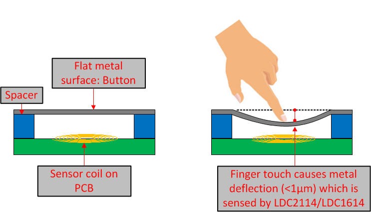 Figure 1 The Working Principle of Inductive Touch
Bending the enclosure will change the inductance and the inductor’s Q factor, which is the inductive reactance at a certain frequency divided by the resistance. An oscillator built out of an inductor and capacitor (LC Oscillator) will change its frequency depending on the bend. The LDC2114 device in Figure 1 can measure the inductance of up to four LC circuits. Another option is the racetrack shaped inductors as shown in Figure 2. The race-track coils give good performance in terms of inductance on the small area.
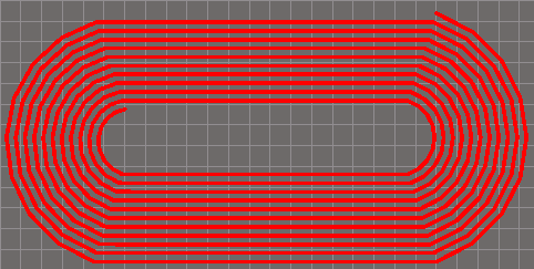 Figure 2 An Example of a Racetrack Coil
Assuring Material Bendability
Material bendability depends on the exposed area, thickness, force and composition. A thin material will bend more than a thicker material; a larger exposed area will bend more than a small area.
Besides material bendability, it’s also important to consider the inductance of the coil. With a large area, you can easily achieve enough inductance to get a good resonant circuit with a frequency below 30MHz. A small area will have a small inductance, which will require increasing the capacitance to keep the resonant circuit’s frequency within the limit. Increasing the capacitance will also decrease the Q factor of the circuit. This inductor-to-digital converter (LDC) configuration tool will help you design your buttons correctly.
The standard evaluation module (EVM) for the LDC2114 is good for testing rather large buttons; I have tested how small you can build such buttons using a standard PCB with 1mm thickness and trace width/spacing of five mil. To test the lowest size, I built a PCB containing two commonly used shapes, such as round coils and racetrack coils in different sizes from 9 to 2 mm. Including the LDC directly on the board eliminates influences caused by cabling between the button and the LDC; otherwise, touching the cable would have more effect than pressing the button. This effect will occur at the high frequencies present with small buttons.
Figure 3 shows the rendered board mentioned above with its spacer. For this test, no special manufacturing capabilities are necessary; it is a standard 1mm-thick FR4 board with 5mil traces and spacing. The spacer is built as a PCB with 1mm thickness and doesn’t contain any traces or anything other than holes. This enables the use of common manufacturing capabilities to test the limits of the technology.
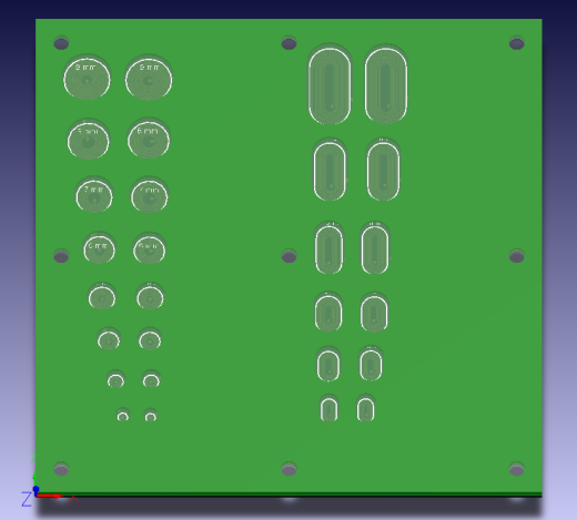 Figure 3 Test Board for Inductive Buttons
The buttons range from 9mm down to 2mm in diameter. The racetrack inductors range from 8mm by 16mm to 3mm by 4.8mm.
Figure 4 shows the assembled test board. Every group of four buttons can connect to the I2C bus of the LDC2114 EVM. Since there are no high frequencies or currents, no precaution with shielded cables is necessary here. Almost every cable can be used without influencing the buttons. Not having cables that might influence your results enables easy and reliable testing of the button design. You can use the software of the downloadable EVM for button configuration and evaluation.
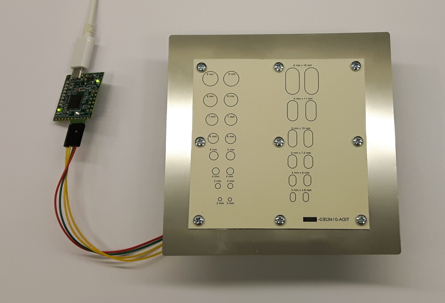 Figure 4 Test Board Hooked up to the LDC2114 EVM
The test shown in Figure 4 uses 120µm-thick stainless steel. To minimized cross-influence and moving of the buttons, a PCB, a PCB as a spacer and the metal cover are screwed together. You could glue everything together, but that would prevent you from testing other materials after gluing one board to a metal plate.
Figure 5 shows the graphical user interface (GUI) that comes with the LDC2114 EVM and the response of one of the buttons. One button generates a large amplitude; the others are only minimally influenced.
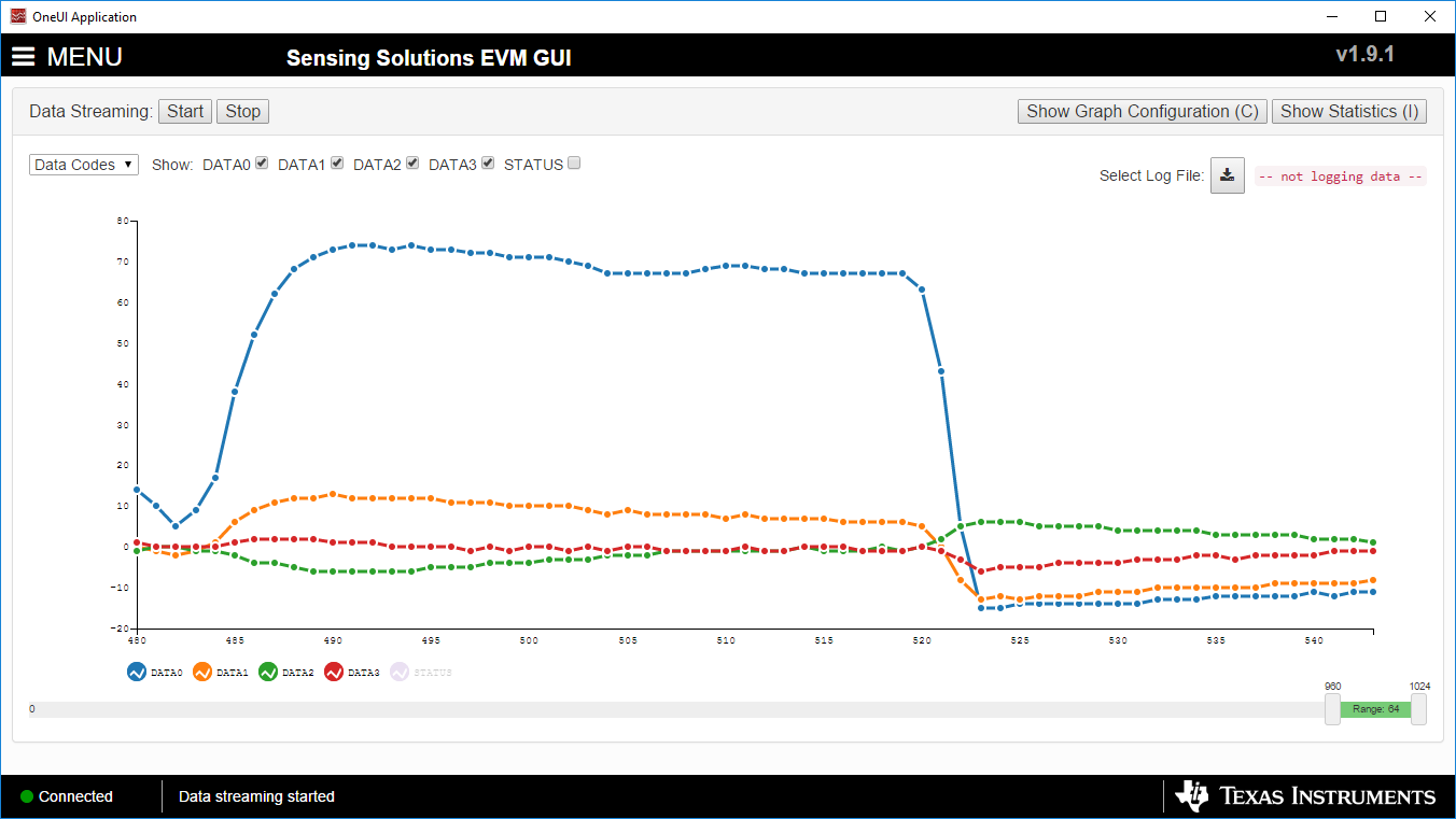 Figure 5 The LDC2114 EVM GUI When Pressing a Button
As expected, the smallest buttons on the board do not work because the 2mm and 3mm diameters are too small and the inductance is too low, so the resonant frequency is too high. Also, a 2mm button is hard to press and will only bend a little. So you cannot use such small buttons with this mechanical design. Although buttons 4mm and larger are large enough to have a resonant frequency that works, buttons of this size are still hard to press, so you might want to use a pen or design an elevation in your housing. The smallest racetrack coils (only 3mm by 4.8 mm) will work for sensing the bending of the material.
Overall Benefits
Building a design for water and dustproof buttons depends on a mechanical bending of metal that cannot be influenced by water (or anything else) and will work when touched with gloves or tools. When a device has to withstand higher temperatures or chemicals, an inductive sensing method for buttons simplifies your design, since no special sealing for the buttons is necessary.
Another benefit of inductive sensing is for tamper detection. Placing a coil on the PCB where the device can be opened can indicate a tamper attack and is more difficult to fool than a mechanical switch because you can place a PCB inductor on your board, right behind the housing. When you now open your device you remove the housing the inductance changes and this can be detected.
So all in all, you can build four buttons out of the housing itself, a simple spacer, one integrated circuit (IC) and a few passive components. This is a highly customizable design that can be waterproof or dustproof.
Additional Resources
- Read the blog post, Modern, sleek and durable touch on metal HMIs.