SSZT728 may 2018 LM5117
Introduction
In a previous blog titled “How to design a simple constant current/constant voltage buck converter,” I discussed how to design a constant current/constant voltage converter (CC/CV). With the addition of a simple modification, the functionality can be modified to regulate the output power and operate within a constant power (CP) limit as the output voltage varies in the CC mode of operation. This blog discusses the simple modification need to design a CC/CP/CV converter using the current monitor (CM) feature of the LM5117 buck controller.
Application Example
In the CC mode of operation, the output voltage increases as the load resistance increases, and as a result, the output power will increase linearly as the current is regulated into the load. However some applications require the output current to be reduced as output voltage increases thereby limiting the power delivered to the load. A relatively flat power limit over a wide output voltage range can be achieved with a simple modification to a CC/CV converter that uses the LM5117.
Method of Implementing CC/CP/CV
Figure 1 shows a typical discrete implementation of a CC/CP/CV converter. The difference between the CC/CV converter and the CC/CP/CV converter is the addition of a feedforward resistor (Rff).
 Figure 1 A Typical Discrete
Implementation of a CC/CP/CV Converter
Figure 1 A Typical Discrete
Implementation of a CC/CP/CV ConverterOutput Current Regulation
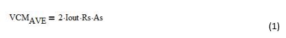
Where Rs is the current sense resistor and As is the internal current sense amplifier gain.
The relationship between the voltage on the CM pin (VCMAVE) and the voltage at the feedback node of the LM5117 (Vfb) is set by the resistor divider network and is expressed in Equation 2.
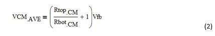
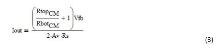
Combining Equation 1 and Equation 2 and rearranging for output current we can see how the output current is controlled by the feedback resistors from the CM to Vfb. This is shown in Equation 3.
CP Programming
Rff has a linear relationship with the output voltage and the output voltage has a linear relationship with Iout. Because we are in effect summing into Vfb, the power limit over a given output voltage range will be nonlinear.
As an example, given the requirements of a 60W power limit and an output voltage range of 6V to 12V, we can calculate the power stage components. It is suggested the power stage components be selected for the highest Iout of 10A corresponding to the lowest output voltage of 6V with a power limit of 60W. From our calculations, we determine Rs = 12mΩ and As = 8.5. Note that the As of the LM5117 is reduced by external 200Ω series resistors at CS and CSG. Refer to the LM5117 datasheet for more details on how series resistors connected to these pins reduces the current sense gain.
As a starting point, select values for RTopCM and RBotCM that will yield a maximum regulated output current 1.4 times greater than the specified regulated current of 10A, which occurs at the minimum output voltage. This suggestion is based on the fact that Rff will reduce VCMAVE as described earlier and therefore reduce Iout.
For example, for a 60 W power limit at a 6 V output, multiply 10 A by 1.4, which yields 14 A of regulated output current. Select 10 kΩ for RBotCM and rearrange Equation 3 to calculate ~25 kΩ for RtopCM. Select a standard value of 25.5 kΩ for RtopCM.
Equation 5 calculates the amount of error introduced at the minimum Vout and serves as a good starting value for Rff:
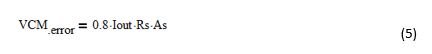
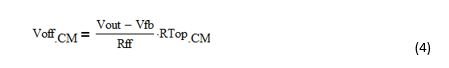
With the addition of Rff at the minimum Vout, you need to ensure that this error is subtracted from VCMAVE by making sure that the VCMerror is equal to the VCMAVE. Make Equation 5 equal to Equation 4 and rearrange for Rff, as shown in Equation 6:
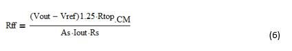
Evaluating Equation 6 yields an Rff = 167kΩ. Select a standard value of 155kΩ for Rff. Using Equation 4, calculate VoffCM = 0.855V at a 6V output.
Equation 7 shows the resulting VCMAVE, which is determined by subtracting Equation 4 from Equation 2:
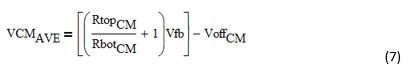
For the given example here, VCMAVE =1.985V
VCMAVE controls the output current and this voltage decreases as the output voltage increases. Equation 8 shows the relationship between the regulated output current (Ioutadj), VCMAVE and VoffCM.
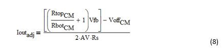
Evaluating Equation 8 yields an Ioutadj = 10.053 at a 6V output.
Multiplying Equation 8 with the output voltage calculates the output power, shown in Equation 9:
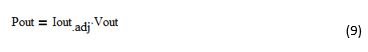
Where
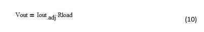
Evaluating Equation 10 calculates a Pout = 60.13W.
I recommend using Equation 7, Equation 8 and Equation 9 to check the power limit for a given output-voltage range to ensure that the power-limit profile suits the needs of your particular application. You can adjust Rff and RTopCM to modify the power-limit profile for a given output-voltage range.
Figure 2 shows a plot of the power limit as voltage increases using the values from the example. As previously stated, the CP regulation is not precisely constant, but the power variation in this example is less than ±7% over the full operating range.
 Figure 2 Power-limit Curve as a
Function of Output Voltage
Figure 2 Power-limit Curve as a
Function of Output Voltage
CC/CP/CV Design of the LM5117
Example Schematic
 Figure 3 Example Schematic for a 5V to 12V Power Limit of 60W and a Voltage Clamp Set at 12.5V
Figure 4 shows the measured efficiency as a function of Iout.
 Figure 4 Efficiency of the Buck Converter Based on Figure 3
Figure 5 shows the measured power-limit profile as a function of the output voltage.
 Figure 5 Power-limit Profile
(I further reduced Rff to keep the power limit below 60W, selecting a final value of 150kΩ for Rff.)
Figure 6 shows the measured output voltage as a function of Iout. The converter’s sense resistor (Rs) sets the maximum current at the right side of the graph. Note that the value of Rs will affect the power-regulation variation.
 Figure 6 Output-voltage Variation as a Function of Iout
Figure 7 shows the measured switch node (CH3), Vout ripple (CH1) and output current (CH4) at 48Vin, 6.6Vout at Iout > 8A.
 Figure 7 Steady-state Scope Shots
Figure 8 shows the measured transient response at a 48V input voltage, with Vout (CH1), Iout (CH4) and a load step from 3.8A to 5.7A (0.1A/µs).
 Figure 8 Transient Response Scope Shots