SSZT784 february 2018 TPD1E04U04
We’ve covered a lot of material in this electrostatic discharge (ESD) fundamentals series, such as the International Electrotechnical Commission (IEC) 61000-4-2 rating, the ESD clamping voltage and junction capacitance. In this final installment of the series, I’ll cover a few more important ESD parameters: reverse working voltage, breakdown voltage and polarity configuration.
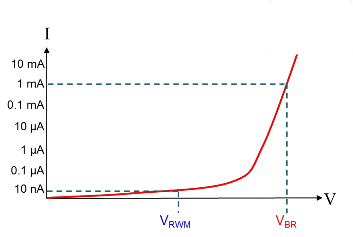
Recall that once the voltage exceeds a certain threshold, the ESD diode will break down and present a low-impedance path to redirect current to ground. During normal operation, however, the ESD diode should be completely “off” and not interfere with the signal or power passing through the trace. This normal operating voltage range is referred to as the reverse standoff voltage or reverse working voltage (VRWM). The VRWM is defined as the maximum positive and negative voltage where current flowing through the diode does not exceed a certain amperage. For several of TI’s newest ESD diodes, this amperage is specified at 10nA. Once the voltage exceeds VRWM, it approaches the breakdown voltage (VBR), which is defined as the voltage where current through the diode exceeds 1mA (Figure 1).
 Figure 1 Logarithmic I-V Curve of an
ESD Diode with vRWM And vBR
Figure 1 Logarithmic I-V Curve of an
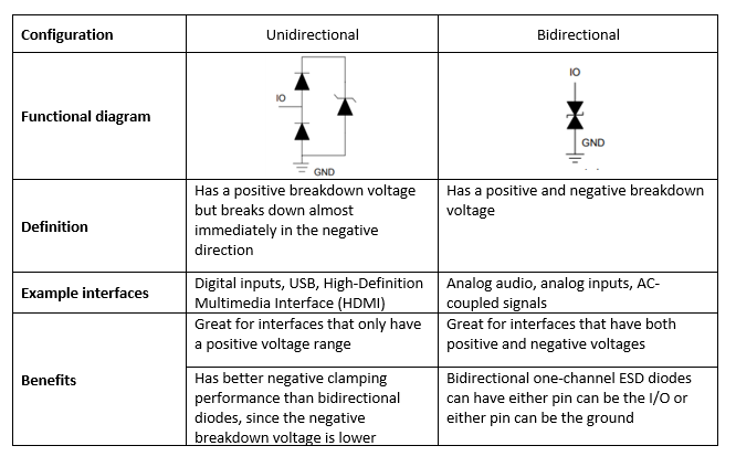
ESD Diode with vRWM And vBRIt is crucial to select an ESD diode with a VRWM that encompasses the interface’s entire voltage range to minimize leakage current during normal operation. When doing this, it is important to pay attention to the polarity configuration of the diode. ESD diodes come in two configurations, as listed in Figure 2.
 Figure 2 Polarity Configuration
Comparison
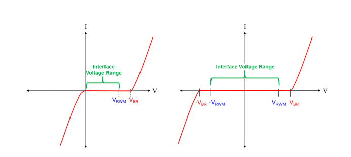
 Figure 3 I-V Curves for a
Unidirectional ESD Diode (Left) and a Bidirectional ESD Diode (Right)
Figure 3 I-V Curves for a
Unidirectional ESD Diode (Left) and a Bidirectional ESD Diode (Right)After covering quite a bit in this ESD fundamentals series, let’s use everything you’ve learned to select a suitable ESD diode to protect a USB 2.0 system that fails at a 19V transmission line pulse (TLP) (here’s a refresher on TLP and clamping voltage).
- USB 2.0 differential signals have a voltage range of approximately 0V (logic low) to 3.6V (logic high), so you want to make sure that your diode’s VRWM encompasses this range.
- USB 2.0 bandwidth can reach up to 480Mbps, so you want to select a diode that has the appropriate capacitance to maintain signal integrity.
- You need to meet IEC 61000-4-2 level 4 compliance, so the ESD diode must be rated for at least 8kV contact discharge and 15kV air-gap discharge.
- The clamping voltage of the ESD diode at a 16A TLP must be less than 19V, since the system will fail at 19V.
The TPD1E04U04 is a good solution because it meets all of these requirements:
- It’s a unidirectional ESD diode that has a VRWM of 0 to 3.6V.
- It has a low capacitance of 0.5pF.
- It has an IEC 61000-4-2 rating of 16kV contact and 16kV air gap.
- The clamping voltage is 9V at a 16A TLP.
This installment concludes the ESD fundamentals series. Feel free to leave a comment below or post on the TI E2E™ Community Circuit Protection forum if you have any questions. Happy ESD hunting!
Additional Resources
- View all articles in the ESD Fundamentals technical article series.
- For more information on ESD selection, check out the “System Level ESD Protection Guide”
- Read Roger Liang’s Analog Applications Journal article, “Design considerations for system-level ESD protection.”
- Check out the application report, “Reading and Understanding an ESD Protection Datasheet.”
- Read the ESD Packaging and Layout Guide.