SSZT802 february 2018 CSD86330Q3D , CSD87331Q3D , CSD87352Q5D
In my last blog post, I talked about how difficult it can be to select the most appropriate field-effect transistor (FET) for switch-mode power supply (SMPS) applications. Predicting circuit performance from a data sheet specification is a tedious process. To get an idea of how tedious, I recommend reading the application note “Power Loss Calculation With Common Source Inductance Consideration for Synchronous Buck Converters,” as it meticulously details the power-loss impacts of first and second order parasitic elements for this one specific topology.
Now, thanks to the Online Design Tools team, TI offers a nifty web-based tool to help you weigh the cost and performance trade-offs for various MOSFETs. The tool uses the equations from the aforementioned application note, and thus only specifically covers a synchronous buck converter topology. However, because this topology is overwhelmingly the most popular non-isolated DC/DC topology for implementing discrete FETs, it still supports a vast array of power-supply end applications.
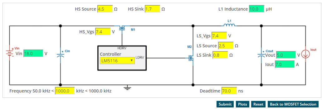
Basically, the tool works as follows. First, a user will select from a list of TI controllers, or build their own controller by entering custom parameters (Figure 1). Then they will enter the various application conditions (input voltage, output voltage, output current and switching frequency if the controller supports that option). And that’s it! From there, the tool does all of the calculations for you!
 Figure 1 Using This Interface, You Can
Input Your End Application’s Parameters and Controller
Figure 1 Using This Interface, You Can
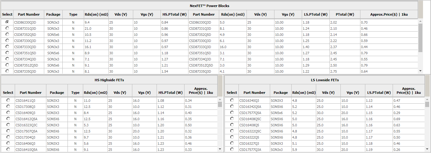
Input Your End Application’s Parameters and ControllerOnce the submit button has been clicked, the tool will determine the minimum FET breakdown voltage that will support the input voltage and rank all potential TI FET solutions by power loss (Figure 2). The higher on the list, the less the power loss for that socket.
 Figure 2 Solutions for the input
parameters shown in Figure 1 ranked by power loss
Figure 2 Solutions for the input
parameters shown in Figure 1 ranked by power lossThe ranked solutions include a list of discrete options as well as power block solutions – a single half bridge vertically integrated into one package. Why would you be interested in power block solutions? In addition to the reduced-footprint and power-density advantages, their stacked-die silicon technology enables an optimized thermal layout and much lower parasitic source inductance compared to two discrete FETs. The application note makes the case that parasitic source inductance can have a significant contribution to total system switching losses, particularly as you drive to higher frequencies. So it’s important that the NexFET power MOSFET selection tool is intelligent enough to account for the secondary effects of common source inductance (LCSI) when calculating loss, because doing so effectively shows some of the measurable advantages of a power block.
I’d like to make a few last points on how the tool should and should not be used. It is most effective as a mechanism for the relative comparison of loss and price (and maybe size). It enables you to quickly assess the trade-offs between solutions firsthand and make the decision most appropriate for you. As an example, let’s refer back to Figure 1 and Figure 2. At first glance, you might select the CSD86330Q3D power block because it is the most efficient of any solution (based on lowest power loss). But look one row down at the CSD87331Q3D and you’ll see a solution that, while 4% higher in total losses, is also 34% cheaper (at 1k quantities). On top of that, the CSD87331Q3D has a 30V breakdown voltage (BVDSS) which will enable greater margin over your 18V input relative to the 25V CSD86330Q3D. Or maybe the designer doesn’t care that the SON3x3 package is smaller; they might be worried about dissipating ~2W into the smaller package due to their end equipment’s hard thermal environment. In that case, maybe they would select the 5mm-by-6mm CSD87352Q5D. The point is that the tool empowers the designer to make the decision themselves.
Under no circumstances should a user assume that the tool is 100% accurate with respect to the loss they will see on your board, because other factors that the tool cannot predict (ambient temperature, board layout considerations) will also impact that final value. Before releasing the tool, the Online Design Tools team did several verification studies and found that predicted losses compared to measured losses were usually within 5-10% – but predicting loss with absolute certainty is not the intention of the tool.
On that point, the tool does remove devices from its ranked recommendations only based upon breakdown voltage considerations. It gives plenty of freedom to design something wildly impractical if one so chooses. For example, there is nothing inherent in the tool that would advise against dissipating 10W of power into a single SON5x6 FET while switching at 10MHz, but good luck trying to get that to work on a real board without melting the printed circuit board (PCB). Although the tool is great at reducing the amount of time and effort that goes into predicting the power loss of dozens of solutions simultaneously, some intelligence on the user’s side is still required to produce a stable design.
I hope you’ll get a chance to play around with this tool the next time you need to select a FET (or power block) device for a buck application, and that you find it as useful and timesaving as I do.
Additional Resources
- Check out the MOSFET Power Loss Calculator User’s Guide, which walks you through using the tool and its various features (it’s even got a plotting function!).
- Ask a question or give feedback in the TI E2E™ Community NexFET Power MOSFETs forum.