SSZT805 february 2018 TLV9061
In my previous blog post, I discussed how low-side current sensing helps control a motor and then provided three steps to design a low-side current-sensing circuit for cost-sensitive applications. In this post, I’ll discuss how you – with the proper printed circuit board (PCB) layout techniques – can design an accurate, low-cost, low-side current-sensing circuit with a single tiny operational amplifier (op amp).
Figure 1 displays the schematic of the low-side current-sensing circuit in my previous blog, shown here using the TLV9061 tiny op amp.
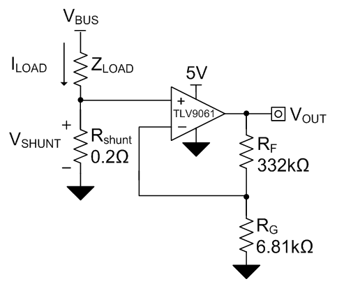 Figure 1 Low-side Current-sensing
Schematic
Figure 1 Low-side Current-sensing
SchematicEquation 1 calculates the transfer function of the circuit shown in Figure 1:
where
There are two main PCB design requirements for an accurate low-side current-sensing design. The first is to ensure that the connections from the shunt resistor are directly connected to the noninverting input of the amplifier and the ground connection of RG. This is typically referred to as a “Kelvin connection.” Not using a Kelvin connection creates a stray resistance in series with the shunt resistor, which causes a gain error in the system. Figure 2 shows the location of the stray resistance in the system.
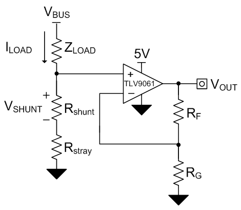 Figure 2 Stray Resistance in Series
with Rshunt
Figure 2 Stray Resistance in Series
with RshuntEquation 2 calculates the transfer function of the circuit in Figure 2:
The second design requirement is to place the ground connection of resistor RG as close to the ground connection of the shunt resistor as possible. As current flows through the ground plane of the PCB, voltage drops develop across the ground plane, which cause voltage differences in the ground plane at different locations on the PCB. These voltage differences cause an offset voltage error in the system. In Figure 3, a voltage source in place of the ground symbol connected to RG represents a difference in ground potential.
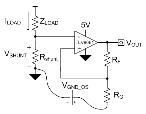 Figure 3 Voltage Differences on the
Ground Plane
Figure 3 Voltage Differences on the
Ground PlaneEquation 3 calculates the transfer function of the circuit shown in Figure 3:
Figure 4 shows a schematic representation of a proper PCB layout.
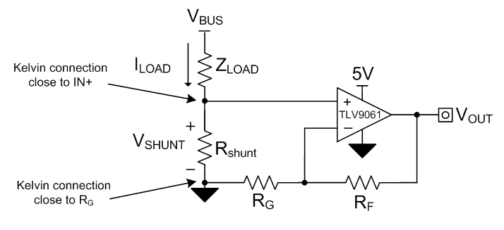 Figure 4 Schematic Representation of a
Proper Layout
Figure 4 Schematic Representation of a
Proper LayoutFigure 5 illustrates proper PCB layout for a low-side current-sensing design following the recommendations I provided earlier. The top layer is red and the bottom layer is blue. R5 and C1 are included in the PCB layout in order to show where you should place a load resistor and decoupling capacitor.
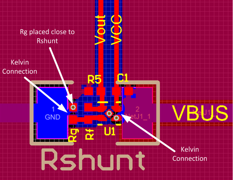 Figure 5 Proper PCB Layout for Low-side
Current Sensing
Figure 5 Proper PCB Layout for Low-side
Current SensingNotice that the traces coming off of Rshunt use a Kelvin connection and RG is placed as close to Rshunt as possible. The TLV9061 op amp’s five-pin extra small outline no-lead (X2SON) package (0.8mm by 0.8mm) enables you to place all passive components in between the two pads of the shunt resistor on the top layer. From there, you can easily use vias to route the connections from the shunt resistor on the bottom layer to the noninverting pin and RG on the top layer.
The next time you lay out a PCB for a low-side current-sensing design, be sure to follow these guidelines to reduce any potential errors in your design:
- Use Kelvin connections on the shunt resistor.
- Place RG as close to the shunt resistor ground as possible.
- Place decoupling capacitors as close to the power-supply pins as possible.
- Pour at least one solid ground plane.
To learn more about designing a PCB layout with the X2SON package take a look at the application report “Designing and Manufacturing with TI’s X2SON Packages.”
Additional Resources
- For additional information on PCB
layout, read these blog posts:
- “The basics: How to layout a PCB for an op amp.”
- “How to layout a PCB for an instrumentation amplifier.”
- Find common analog design formulas in the “Analog Engineer’s Pocket Reference.”
- Read about issues related to decoupling capacitors in amplifier expert Art Kay’s blog post, “The decoupling capacitor … is it really necessary?”
- Learn more in this Planet Analog article, “When GND Isn’t GND, Single-Ended Circuits Become Differential.