SSZT937 october 2017 LM7705 , OPA837
Designers often run into the problem of selecting one of two (or several) inputs to pass on to the next stage. While a plethora of multiplexer (mux)-type devices use a modified impedance approach to select which input passes to a single output, a new high-speed precision operational amplifier (op amp) adds this capability internally.
The OPA837 single-channel op amp includes a switch internal to the inverting node that operates along with the power shutdown feature. This enables simple active-mux operation, shown as the 2x1 example in Figure 1. The extremely low power operation of the 105MHz OPA837 device adds little to the system power budget (0.6mA/channel), while giving almost perfect isolation between channels and in the off-channel path.
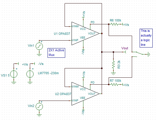 Figure 1 Simple gain of 1, 2x1 active
mux using two OPA837 op amps
Figure 1 Simple gain of 1, 2x1 active
mux using two OPA837 op ampsIn Figure 1, the two amplifiers are shown as a unity gain buffer. They can be configured in any gain or attenuation setting, but in addition to the output load, each amplifier will need to drive a parallel combination of the feedback and gain resistors for both channels.
The power shutdown feature operates off the negative supply. The LM7705 switched capacitor inverting regulator provides a fixed -0.23V negative bias supply voltage from a 3V to 5.25V input to give the necessary headroom on the output to operate true swing to ground. The OPA837 inputs are negative rail. A low-voltage ground-referenced logic signal and its inverted version will toggle between the two amplifiers, making one active at a time. Use break-before-make logic sequencing to avoid both outputs being active at the same time. If break before make is not possible, isolate the two outputs from high transition currents with 100Ω resistors in the outputs inside the feedback connection.
Pulling the power disable voltage below 0.32V on one channel will disable it, while raising it above +1.27V on the other will enable that channel. The -0.23V negative supply provided by the LM7705 has shifted these power disable voltage levels below the minimum/maximum range specific in the data sheet.
The rail-to-rail output stages used in the OPA837 go high impedance when disabled. What has been missing to make this active mux application work is a similar high impedance looking into the disabled channel’s inverting input pin. The OPA837 unity-gain stable voltage feedback op amp (VFA) is the first to provide an active switch to either connect or isolate the internal input stage transistor on the inverting input from the external world. When active, this switch is low impedance and inside the feedback loop, and thus transparent to normal op amp operation. The noninverting inputs remain very high impedance whether enabled or disabled.
A critical test of this active mux capability is a sweep of harmonic distortion for a simple single amplifier case, and then repeating that test with a disabled OPA837 connected to the active stage output. All previous amplifiers showed a nonlinear load vs. output voltage swing (Vpp) into the inactive inverting input, degrading harmonic distortion performance. Figure 2 and Figure 3 show the transparent operation provided by this new active mux at 2Vpp I/O and 4Vpp I/O, respectively. The 4Vpp test (0V à 4V input) required a +5.2V supply to provide 1.2V of headroom at the input stage.
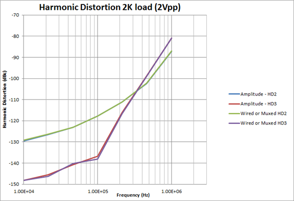 Figure 2 2Vpp with and without an
Inactive Stage Connected to the Output Pin
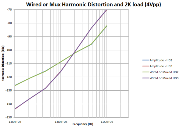 Figure 3 4Vpp with and without an
Inactive Stage Connected to the Output Pin
Figure 3 4Vpp with and without an
Inactive Stage Connected to the Output PinAs these tests show, there was no degradation in harmonic distortion from the simple single amplifier test case.
How else could you use this new internal capability? Here are a few ideas:
- Fan the active mux application to more than a 2x1. For a gain of 1, I recommend a capacitive load-isolating resistor in the feedback to limit the buildup of capacitive load on the active channel output. The parallel inactive inverting input capacitive loads can begin degrading the phase margin for the active channel.
- Take a single source signal and create a simple n-bit digital variable gain amplifier (DVGA) by connecting the outputs of two or more OPA837 stages at different gain settings and selecting only one to be active at a time.
Selectable gain application of the input switch within the OPA837 shows a simple 1-bit DVGA providing a gain of 1 or 2 to the output from a shared input signal.
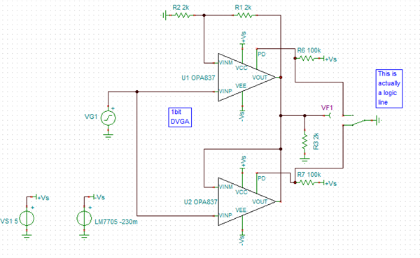 Figure 4 Selectable gain application of
the input switch within the OPA837
Figure 4 Selectable gain application of
the input switch within the OPA837When either path is active, the amplifiers will now need to drive the 4kΩ feedback load in parallel with the 2kΩ load shown in Figure 4. Figure 5 shows the two possible frequency response curves for Figure 4. Of course, a wider gain step is possible by setting one channel to a gain higher than 2V/V. There will be an increasing difference in bandwidths by doing that, however. A post-filter lower than the lowest stage bandwidth will hold the response shapes constant as different gain channels are selected.
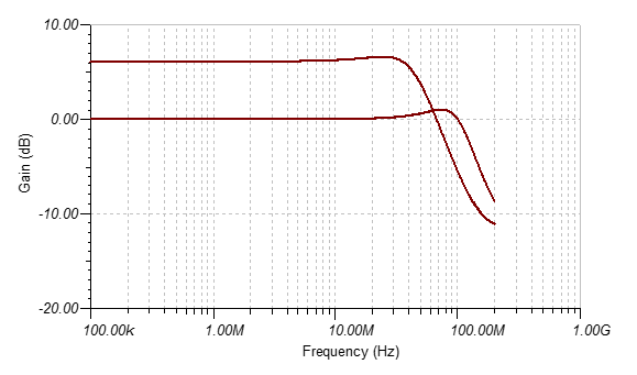 Figure 5 1-Bit DVGA Small-signal
Response Shapes for a Gain of 1 and 2 in the OPA837
Figure 5 1-Bit DVGA Small-signal
Response Shapes for a Gain of 1 and 2 in the OPA837You can use the OPA837 to solve your simple mux problems, adding some gain in the signal path if desired. Or you could extend your dynamic range by using the OPA837 to provide a simple switched gain stage. Both applications are well supported by the exceptional DC precision and low power of the OPA837. Learn more about single mux design in the E2E™ High Speed Amplifiers forum.
Additional Resources
- Download the OPA837 and LM7705 datasheets.
- Check out the ADC Voltage Reference Buffer Optimization Reference Design for High Performance Data Acquisition Systems.
- Start designing quickly with the OPA837 evaluation module (EVM).