SSZT980 august 2017 TMS320F28027
You probably don’t reach for an oscilloscope first when debugging an analog-to-digital converter (ADC) integrated into a microcontroller (MCU). But an oscilloscope can help you make sure that the ADC operates as expected. In this blog post, I’ll use the C2000™ Piccolo™ F28027 MCU as an example to show you how.
The precise timing of the ADC is important, especially for closed-loop control systems such as digital power supplies or motor-control applications. In theory, the task is very simple – use the data sheet to configure the ADC according to the system requirements. However, peripherals integrated into MCUs are more and more complex and developers have to be careful readers and not misinterpret the data sheet.
An operational amplifier (Figure 1a) or a resistor divider (Figure 1b) typically drives the input of the ADC. A simplified model of the ADC input has switch resistance (RON), a sample-and-hold capacitor (CH) and parasitic input capacitance (CP). During the sampling period, when the switch (SW) conducts, in-rush current flows through the ADCIN pin in order to charge CH to the input voltage level. This results in a voltage drop on the ADCIN pin due to the current-limiting output impedance of the signal source.
It is a good engineering habit to add a charge bucket filter (R1, C1). The capacitor in the bucket filter acts as a charge reservoir for CH and helps to reduce the voltage drop on the ADCIN pin during the sampling process to a reasonable level (typically 5% of the reference voltage). This filter has a cut-off frequency way above the sampling frequency and is not intended to serve as the anti-aliasing filter. (For more details about charge bucket filter design procedures, see the 16-Bit 1-MSPS Data Acquisition Reference Design for Single-Ended Multiplexed Applications.)
 Figure 1 TMS320F28027 ADC input driven
by an operational amplifier (a); and a resistor divider (b)
Figure 1 TMS320F28027 ADC input driven
by an operational amplifier (a); and a resistor divider (b)Figure 2 shows how you can benefit from the usually unwanted effect of voltage drop during the analog-to-digital conversion. The Bidirectional DC/DC Converter Reference Design for 12-V/48-V Automotive Systems uses a C2000 MCU for the voltage feedback loop. The application requires precise control-loop timing including the analog-to-digital conversion. The ADC in the MCU enables automatic sequential sampling of multiple channels, where each channel can have different sample-and-hold time or priority. This results in a complex configuration of multiple registers, which is not trivial.
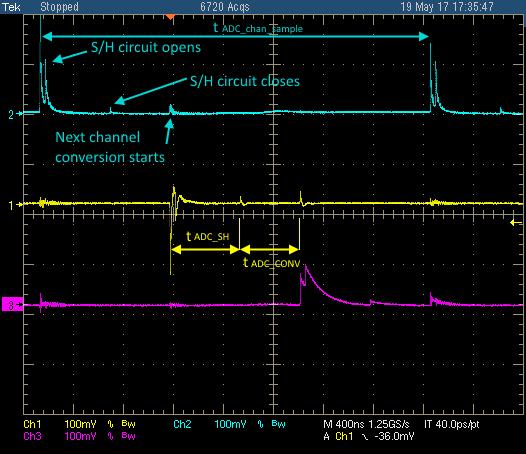
Figure 2 shows the configuration of the ADC for the bidirectional reference design, with three channels (ADCINA1, ADCINA3, and ADCINB7) sampled sequentially. The clock source for the ADC runs at 25MHz, which corresponds to 40ns per cycle. The sample-and-hold time (tADC_SH) is set to 12 cycles (480ns) and the conversion time (tADC_CONV) is fixed to 13 cycles (520ns); therefore, the complete conversion takes 1µs per channel. Each channel is sampled every 3µs.
 Figure 2 Analog-to digital conversion
timing for the bidirectional DC/DC converter reference design
Figure 2 Analog-to digital conversion
timing for the bidirectional DC/DC converter reference designIn the reference design, the TLV2272-Q1 operational amplifier drives the ADCINA1 and ADCINA3 inputs (as shown in Figure 1a), whereas a resistor-capacitor (RC) network drives the ADCINB7 input (as shown in Figure 1b). In order to verify the configuration, C1 is removed from all three channels (the first version of the reference design did not implement a bucket filter for ADCINA1 and ADCINA3).
Figure 3 shows ADCINA1, ADCINA3 and ADCINA7 waveforms measured with a Tektronix TDS5054B oscilloscope and Tektronix P5050 low-cost 10X (typically 10MΩ/11.1pF) passive probe. The oscilloscope is set to high-resolution mode. All channels are AC-coupled and the bandwidth is limited to 200MHz.
 Figure 3 ADCINA1 (channel 2), ADCINA3
(channel 1) and ADCINA7 (channel 3) waveforms in the bidirectional reference
design
Figure 3 ADCINA1 (channel 2), ADCINA3
(channel 1) and ADCINA7 (channel 3) waveforms in the bidirectional reference
designSignal peaks clearly indicate the tADC_SH and tADC_CONV period on every individual channel. Even the end of the analog-to-digital conversion is visible when the sample-and-hold circuit reconnects to the consecutive analog channel. The positive character of the peaks implies that the signal voltage level of the foregoing channel was higher and CH discharges back to the circuit. The absolute value and shape of the peaks are not relevant because the oscilloscope probe significantly affects the overall capacitance on the ADCIN pin. In order to obtain an accurate voltage level, you must use an active oscilloscope probe with minimal input capacitance.
Success Story
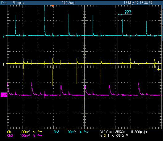
Five minutes in the lab helped identify the bug shown in Figure 4. According to F28027 errata, the first ADC sample at the beginning of every series may be corrupted. One solution is to add an extra conversion in the series and discard the first result. Another solution is to change the timing of the ADC by disabling overlap mode and reducing the ADC clock to a maximum of 30MHz. I initially attempted the first solution, but decided to use the second solution. However, I did not change my source code properly and the extra conversion remained in the code flow. After removing the extra line of code, the ADC operates identically to Figure 2.
 Figure 4 Unexpected conversion every 10 cycles
Conclusion
The technique I’ve laid out here uses inexpensive equipment and gets you one step further in designing reliable, high-performance and robust applications. For additional information, download the code snippet I used for this example below (text file).