SSZT999 august 2017 TLV9062
Capacitive loads can cause stability problems in operational amplifier (op amp) circuits, resulting in large overshoots, ringing, long settling times – and in severe cases, sustained oscillations. These issues occur because the capacitive load interacts with the op amp output impedance, forming an additional pole in the open-loop gain (Aol) response that reduces the loop-gain (Aol*β) phase margin below acceptable levels.
Many resources present basic stability theory in great detail, including TI Precision Labs’ videos on op amp stability. There are different compensation circuits which allow the op amp to remain stable while driving the capacitive load. In this blog post, I’ll review three common compensation circuits that can be designed and tested using the do-it-yourself amplifier evaluation module (DIYAMP-EVM).
Isolation Resistor – RISO
The most common and easiest-to-design method places an isolation resistor (RISO) in series with the capacitive load. The isolation resistor adds a zero to the Aol*β transfer function, which cancels the phase shift from the pole and returns the rate of closure (ROC) to 20dB/decade. As shown in Figure 1, this compensation circuit produces stable results with phase margins greater than 60 degrees by following the design steps in the TI Precision Labs videos and placing the zero at or above the frequency where the loaded Aol curve is equal to 20dB. Moving the zero higher in frequency lowers the phase margin to achieve a more critically damped response. The main disadvantage to this compensation method is that there will be a voltage drop across RISO, which reduces the DC accuracy of the circuit when driving a load.
 Figure 1 RISO capacitive load compensation circuit and open-loop results
RISO + DFB Circuit
A common solution to maintain DC accuracy while stabilizing the load is to use the RISO plus dual-feedback (RISO + DFB) circuit. As the name suggests, this compensation circuit has two feedback paths. There is a DC feedback path through RF that regulates the voltage at the load and an AC feedback path through CF, which makes the circuit act like the RISO circuit at high frequencies to stabilize the capacitive load. Be sure to follow the guidelines in the TI Precision Labs videos for setting the feedback components to achieve proper operation.
 Figure 2 RISO + DFB compensation circuit and open-loop results
RISO + DFB + RFx Circuit
Another compensation method that maintains DC accuracy but offers improved transient response is the RISO + DFB + RFx circuit. This circuit is basically the same as the RISO + DFB circuit with an additional resistor, RFx, in series with CF. The addition of RFx will cause the circuit noise gain (1/β) to increase and flatten off at higher frequencies to a magnitude of 1 + RFx/RF. This increase in noise gain can be helpful to compensate difficult capacitive loads, lower the loop-gain crossover frequency, adjust the phase margin and shape the closed-loop output impedance. For this circuit to be stable, the 1/β response must flatten off to the high-frequency level before it intersects with the Aol curve to achieve a 20dB/decade ROC. Figure 3 shows the Riso + DFB + RFx circuit and the open-loop results.
 Figure 3 RISO + DFB + RFx Compensation Circuit and Open-loop Results
Figure 4 compares the transient results to a small-signal step input at both the op amp output (Vo) and the circuit output (VOUT). The RISO circuit displays a typical overdamped response with a moderate settling time. The RISO + DFB circuit output has a rounded single-lobe overshoot and long settling tail resulting in slower settling times than the RISO circuit. The RISO + DFB + RFx output has a sharp single-lobe overshoot but settles very quickly to the final output value with a similar settling time to the original RISO circuit.
While the overshoot spike at the op amp output in the RISO + DFB + RFx circuit (Vo_RFx) looks troubling, the behavior is a result of the complex nature of this circuit’s transfer function and how the placement of the poles and zeros affects the transient response. Don’t worry; the circuit is stable. The overshoot is aperiodic and not followed by the substantial ringing that would normally be associated with this level of overshoot if the circuit was unstable.
 Figure 4 Comparison of Small-signal Step Responses for the Three Compensation Circuits
Figure 5 compares the total output noise of the three circuits. The RISO circuit has the lowest noise, followed by the RISO + DFB circuit and then the RISO + DFB + RFx circuit. The RISO + DFB + RFx circuit has the highest noise because of the increase in noise gain at higher frequencies. Circuits with higher ratios of RFx/RF will have more noise than those with smaller ratios.
 Figure 5 Total output-noise comparison for the three compensation circuits
You can evaluate all three of these circuits using the RISO + DFB circuit in the DIYAMP-EVM shown in Figure 6. Table 1 lists the component configurations to create each of the three circuits using the DIYAMP-EVM RISO + DFB circuit.
 Figure 6 RISO + DFB Circuit in the DIYAMP-EVM
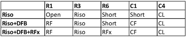 |
I hope that after reading this post, you’ll feel confident doing your own stability analysis and compensation using the DIYAMP-EVM.
Additional Resources
- Check out the DIYAMP-SOIC-EVM User’s Guide.
- Check out the Dual-Channel DIY-AMP EVM.
- Download the Analog Engineer's Pocket Reference Guide
- Learn more about the TLV9062 op amp.