SSZTA96 April 2017 TPS543C20
The peak voltage at phase node, VPH, in a synchronous buck converter is one of the main specifications to determine converter reliability. Designers usually allow phase-node ringing to be as much as 85% to 90% of the MOSFET data sheet’s absolute maximum rating. This margin is necessary for long-term reliability of the converter since the circuit needs to safely operate over a wide range of ambient temperature (-400C to + 850C).
From the driver side, the main factor contributing to phase-node ringing is the gate-driver strength during the turn-on process of the upper MOSFET, FETUPPER. Let’s analyze its effects in a converter with different gate-driver resistance values.
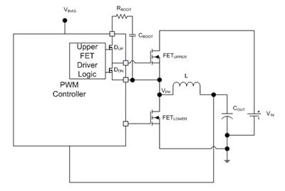
Figure 1 shows the top level of a synchronous buck converter with the upper MOSFET gate-driver section. The FETUPPER requires a charge to turn on. This charge comes from the boot capacitor, CBOOT. The charging path starts from CBOOT, to RBOOT, to the pull-up driver P-MOSFET (DUP), the FETUPPER input capacitor and back to CBOOT.
 Figure 1 Top-level Synchronous Buck Converter
To simplify the comparison, treat RBOOT as a short and assume MOSFET DUP behavior as a linear resistance during the turn-on period of the FETUPPER. A higher DUP resistance value has a lower peak ringing voltage and lower converter efficiency due to higher switching power losses. A lower resistance value has both a higher peak-ringing voltage and better efficiency.
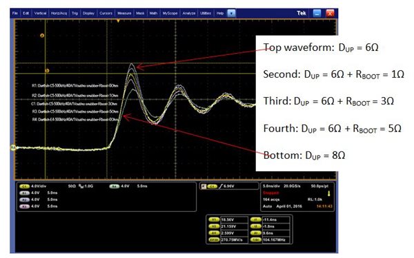
Figure 2 shows the rising edge of phase-node ringing with different gate-driver strength values. The waveforms are from the TPS543C20 evaluation board with VIN =12V, VOUT =1V, FSW = 500 kHz, ILOAD = 40A on. The peak ringing voltage of 6Ω DUP is about 6V higher than 8Ω DUP. The resistance value of DUP inside the TPS543C20 can be program via an external communication interface such as an I2C protocol. The waveforms are from the same device and same evaluation board to minimize variation from other components.
Now, let’s compare a 6Ω DUP along with different boot resistor values to an 8Ω DUP. From the first order of the circuit analysis, a 6Ω DUP along with a 2Ω boot resistor should have the same peak ringing voltage as the 8Ω DUP. Figure 2 also compares the 6Ω DUP value with 1Ω, 3Ω and 5Ω boot resistors. The peak ringing voltages of these configurations are higher than the 8Ω DUP value.
You might ask why the 6Ω DUP with a 2Ω boot resistor and the 8Ω DUP values do not have the same peak ringing voltage results. This is because the DUP behaves as a dynamic MOSFET, which requires time during the turn-on process, in comparison to pure resistance as RBOOT. As a result, the rising slope of a phase node with a 6Ω DUP and 6Ω DUP plus boot resistors has the same ratio and is faster than the 8Ω DUP slope.
 Figure 2 Phase-node Ringing on the TPS543C20 Device
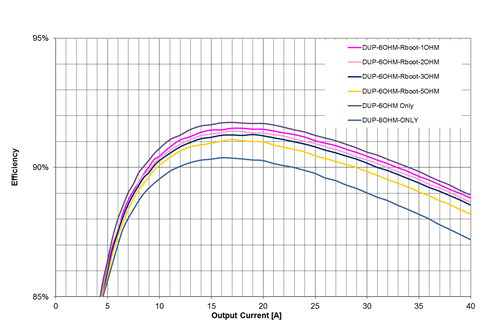
Figure 3 compares the efficiency of all configurations. The results clearly correlate our earlier assessment. 6Ω DUP efficiency is the highest and has the highest peak voltage ringing. And, 8Ω DUP efficiency is the lowest with the lowest peak voltage ringing.
 Figure 3 Efficiency Comparison with Gate-driver Strength Variation
It’s critical to optimize the gate-driver strength with the main power-stage MOSFETs to ensure reliability and obtain the highest converter efficiency. A small variation in gate-driver strength can lead to wide variations in converter performance. Consider the TPS543C20 fixed frequency, non-compensation stackable synchronous buck converter for your next design.