SSZTAE3 february 2017 LM34936 , LM5175 , LM5176 , LM5176-Q1
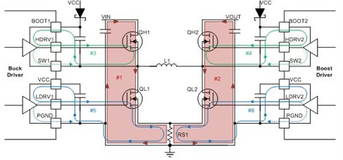
As I discussed in my previous blog, layout is very critical to the success of a buck-boost converter and the first step is identifying the critical components. Once you have identified the critical parts of your DC/DC converter design, your next task is to minimize any sources of noise and unwanted parasitics. Minimizing hot loops is a major first step in this direction. Figure 1 shows the hot loops or high di/dt loops in a four-switch buck-boost converter. Figure 1 also highlights the hot loops formed by the gate drives and their return paths, in addition to the input and output switching loops (Nos. 1 to 6).
 Figure 1 Hot Loops in a Four-switch
Buck-boost Converter
Figure 1 Hot Loops in a Four-switch
Buck-boost ConverterSince the power-stage hot loops (in red) contain the largest switching currents, optimize these first. The input loop (No. 1) carries the switching current when in buck cycles. The output loop (No. 2) carries the switching current when in boost cycles. In my experience, I’ve realized the lowest loop area and the most compact design when optimizing both loops using a symmetric layout.
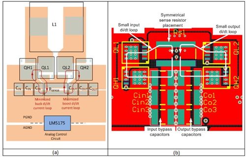
Figure 2 and Figure 3 are examples of good power-stage layouts. The layout example shown in Figure 2a provides a better thermal path for the heat generated in the sense resistors and the FETs to spread. Consider following the layout example shown in Figure 2b to create higher-density designs, as it packs the power-stage components closer together.
 Figure 2 A Symmetrical Power-stage
Layout Minimizes Both the Input and Output Power Loops in a Four-switch
Buck-boost Converter, (a) Medium Density Design, (b) High Density Design
Figure 2 A Symmetrical Power-stage
Layout Minimizes Both the Input and Output Power Loops in a Four-switch
Buck-boost Converter, (a) Medium Density Design, (b) High Density DesignThere is a trade-off in size, thermal robustness and noise performance of the power stage. Smaller di/dt loops and smaller dv/dt nodes have lower parasitics and also radiate less. They are also more robust in the presence of external noise, as smaller loop areas couple less noise. Smaller designs are more constricted thermally, however, because there isn’t much copper directly connected to the heat-dissipating elements, which include MOSFETs, sense resistors and the inductor. For relatively higher-power designs, you may need extra copper area at the switch nodes to limit the temperature.
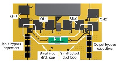
Figure 3 shows a design capable of handling higher currents and allows for the paralleling of FETs. The heat is distributed between the FETs, which can then spread to adjacent copper planes and thus avoid excessive temperature increases or the formation of hot spots.
 Figure 3 An Example Layout with
Parallel FETs and Larger Copper Areas for Higher-power Designs
Figure 3 An Example Layout with
Parallel FETs and Larger Copper Areas for Higher-power DesignsIn the next installment of this series, I will discuss how to optimally route sense connections.