SSZTAJ6 december 2016 UCC24636 , UCC28704
With the increased interest in energy efficiency and energy conservation, a synchronous rectifier (SR) helps boost efficiency when converting offline AC power into 5V for USB smartphone battery charging. During this conversion, an SR controller integrated circuit (IC) needs proper biasing in order to provide the adequate drive to the SR MOSFET. The bias voltage is typically above 4V in USB applications. Because the BC1.2 USB battery-charging standard specifies a power adapter output in the range of 4.1V to 6V, you can bias SR controller ICs from that output, as shown in Figure 1.
 Figure 1 Flyback Converter with the SR Controller Biased from the Output Voltage
What If the Output Voltage Drops below UVLO?
 Figure 2 Typical 5V-3A Power Adapter Output Characteristics
When the output drops below 4V, the SR turns off, which causes undesired performance. First, the SR turn-off causes a constant current shift due to the voltage increase from the body-diode conduction, leading to unnecessary transients. Second, the current flowing through the SR MOSFET (QSR) channel now flows through its body diode. The resulting higher-power losses may cause a temperature rise that could cause thermal runaway and damage. Therefore, you need alternative approaches to keep the SR on before the output drops to 3V.
Biasing an SR Controller Using a Charge Pump
 Figure 3 Charge-pump Biasing
Biasing an SR Controller Using a Linear Regulator
 Figure 4 Pulse Linear-regulator Biasing
Biasing an SR Controller Using a Simple Regulator
 Figure 5 Simple Regulation Bias
The bias VDD pin accepts a wide voltage range from 4V to 30V – and the driver output is internally clamped to the MOSFET’s gate-voltage level, 10V. These features enable a simple regulator (placed externally with a diode and a resistor) to charge the VDD capacitor to a proper level across the input and load range. When the drain pin voltage is pulsing, the diode (D) rectifies the pulses, while the resistor (R) and capacitor (C) average out the pulses to deliver DC voltage and power to VDD.
Table 1 provides biasing results based on the TI Designs Universal AC Input to 5V/3A Output Reference Design, which employs the UCC28704 and UCC24636, a universal offline input, and a 5V-3A output flyback converter.
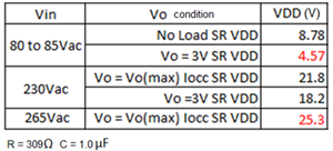
|
The results depict a minimum controller VDD voltage above 4.57V even if the converter output drops to 3V, thus maintaining plenty of bias voltage to keep the UCC24636 in operation.
When converting offline AC power into 5V for USB smartphone battery charging, an SR controller can help boost efficiency when biased properly.
Additional Resources:
- Read the blog post: USB Type-C: charging a new world
- Discover more about the UCC28704:
- UCC28704 user guide
- Get to know the design tools for the UCC28704, including a SPICE model, WEBENCH® Designer calculator, Excel calculator, MathCAD calculator