SSZTAX0 september 2016
Have you ever had to do the same calculations more than once? As an electrical/electronics engineer, I am pretty sure that you have. If you are doing calculations manually, it can be quite tedious and very time-consuming. When designing power-management circuits, you can change a lot of parameters and choose from a whole variety of topologies, which can increase the amount of repetitive calculations.
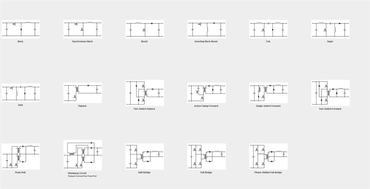
The brand-new Power Stage Designer Tool 3.0 calculates the necessary voltage and current information for 17 power-supply topologies instantly. In Figure 1 you can see the topologies, which are supported. There is no need to wait for results after entering your inputs – as you would have to with a simulation – because the tool is based on equations, assuming perfect coupling and considering only diode losses. This means that you should pick your components with a reasonable margin so that effects like ringing or spiking caused by parasitics won’t cause any damage in the final design.
The tool also displays waveforms for all of the important components of the power stage. If you are not yet familiar with a topology, Power Stage Designer can also help you understand its mode of operation. The tool can calculate results and waveforms both in continuous conduction mode (CCM) and discontinuous conduction mode (DCM) for 14 topologies. The synchronous buck, Weinberg and phase-shifted full-bridge topologies are only available in CCM.
 Figure 1 Topology Overview of Power
Stage Designer 3.0
Figure 1 Topology Overview of Power
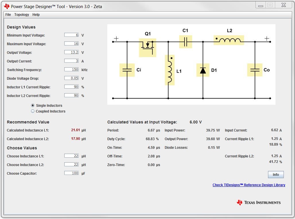
Stage Designer 3.0Figure 2 shows the information available in the main window exemplified by the Zeta converter main window.
 Figure 2 Zeta Converter Main
Window
Figure 2 Zeta Converter Main
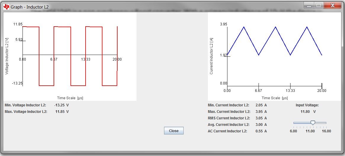
WindowYou can view the peak values for currents and voltages, root-mean-square (RMS) current, alternating current (AC) and waveforms for each component individually by clicking on its symbol in the schematics. This information, like displayed in Figure 3 for L2 of a Zeta converter, enables you to choose the appropriate device rating and number of components for your design. After all, the components you choose need to be able to withstand current and voltage stress under all specified conditions. A slider in the graph window enables you to alter the input voltage within the entire input-voltage range. Calculations are independent of a specific controller, which gives you the flexibility to evaluate different topologies first. Thus, you will get a good overview without already having to dig too deep into data sheets during the beginning of the design phase. Of course, after picking a topology and a controller/converter, you have to make sure that your inputs do not violate certain integrated circuit (IC) limits, such as minimum on time, off time or maximum duty cycle.
 Figure 3 Graph Window for L2 of the
Zeta Converter
Figure 3 Graph Window for L2 of the
Zeta ConverterWhen you are happy with your design and want to keep the parameters, you can save your setup in a file and load it again whenever you need it. Another option is to search TI’s website for already built and tested TIDesigns, which might match your specification. Or just transfer the design parameters to WEBENCH® Design Center, where you can look for a controller/converter and optimize your design.
Additional Resources
- Check out Power Stage Designer 3.0 and enjoy designing faster and much more conveniently.
- Watch our latest training video: Introduction to Power Stage designer