SSZTB92 may 2016 TPS548D22

Residents seeking more space generally give up living near downtown areas, with their likely proximity to work and city services, and move to the suburbs for bigger homes and spacious yards. Similarly, when engineers require higher currents for their point of load (POL) designs, they generally give up the conveniences of high-density converters (with integrated MOSFETs) and instead use a more sprawling solution involving controllers (with external MOSFETs). Controllers, like the suburbs, can offer relative flexibility and affordability, but take up more real estate – more board space, that is.
Until recently, applications requiring currents in excess of 10-15A generally relied on controllers with external MOSFETs. Converters – while enabling simpler designs with easier layout, fewer components in their bill of materials (BOM) and higher-density solutions with high reliability – traditionally delivered only a limited amount of power.
Applications such as network routers, switches, enterprise servers and embedded industrial systems are increasingly power-hungry – requiring 20A, 30A, 40A or more for their POL design. Yet these applications are extremely space-constrained and it is difficult to accommodate solutions involving controllers and external MOSFETs. The question is, how do you use converters rather than controllers in an application with large current requirements?
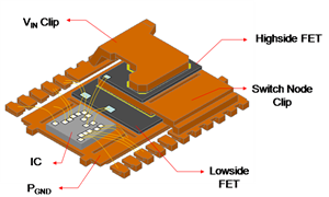
The answer primarily lies in recent advancements in MOSFET and packaging technologies. New-generation MOSFETs like TI’s NexFET™ power MOSFET offer lower resistivity (Rdson) in a given silicon area for higher current capability. PowerStack™ packaging technology stacks the integrated circuit (IC) and MOSFETs on top of one another – resembling a downtown building – to pack more in a given footprint.
 Figure 1 Controller IC and MOSFETs
Vertically Stacked in the PowerStack Package
Figure 1 Controller IC and MOSFETs
Vertically Stacked in the PowerStack PackageThe unique combination of die stacking and clip bonding in PowerStack packages results in a more integrated quad flat no-lead (QFN) solution that delivers a smaller size, better thermal performance and higher current capabilities over traditional solutions that place MOSFETs side by side.
With recent advances in MOSFET and packaging technologies, TI now offers the option of using converters - with integrated FETs - for high-power, high-density POL applications. The TPS548D22 joins TI’s family of high-current synchronous SWIFT™ DC/DC buck converters to deliver up to 40A of continuous current and is offered in a 40-pin 5mm-by-7mm-by-1.5mm stack-clipped QFN PowerStack package. Visit the DC/DC portal for the comprehensive TI offering. Those of you who had to move to the suburbs can now consider moving back downtown!