SSZTBC4 May 2016 OPA855 , OPA858 , OPA859
Transimpedance amplifiers (TIAs) act as front-end amplifiers for optical sensors such as photodiodes, converting the sensor’s output current to a voltage. TIAs are conceptually simple: a feedback resistor (RF) across an operational amplifier (op amp) converts the current (I) to a voltage (VOUT) using Ohm’s law, VOUT = I × RF. In this series of blog posts, I will show you how to compensate a TIA and optimize its noise performance. For a quantitative analysis of a TIA’s key parameters, such as bandwidth, stability and noise, please see the application note, ““Transimpedance Considerations for High-Speed Amplifiers.”
In a physical circuit, parasitic capacitances interact with the feedback resistor to create unwanted poles and zeros in the amplifier’s loop-gain response. The most common sources of parasitic input and feedback capacitances are the photodiode capacitance (CD), the op amp’s common-mode (CCM) and differential input capacitance (CDIFF), and the circuit-board capacitance (CPCB). The feedback resistor, RF is not ideal and has a parasitic shunt capacitance that may be as large as 0.2pF. In high-speed TIA applications, these parasitic capacitances interact with each other and RF to create a response that is not ideal. In this blog post, I will illustrate how to compensate a TIA.
Figure 1 shows a complete TIA circuit with parasitic-input and feedback-capacitance sources.
 Figure 1 TIA Circuit Including
Parasitic Capacitances
Figure 1 TIA Circuit Including
Parasitic CapacitancesThree key factors determine the bandwidth of a TIA:
- Total input capacitance (CTOT).
- Desired transimpedance gain set by RF.
- The op amp’s gain-bandwidth product (GBP): the higher the gain bandwidth, the higher the resulting closed-loop transimpedance bandwidth.
These three factors are interrelated: for a particular op amp, targeting the gain will set the maximum bandwidth; conversely, targeting the bandwidth will set the maximum gain.
Single-pole Amplifier with No Parasitics
The first step of this analysis assumes an op amp with a single pole in the AOL response and the specifications shown in Table 1.
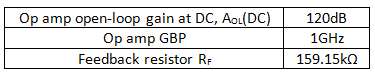
|
An amplifier’s closed-loop stability is related to its phase margin, ΦM, which is determined by the loop-gain response defined as AOL × β, where β is the inverse of the noise gain. Figure 2 and Figure 3 show the TINA-TI™ circuits to determine the op amp’s AOL and noise gain, respectively. Figure 2 configures the device under test (DUT) in an open-loop configuration to derive its AOL. Figure 3 uses an ideal op amp with the desired RF, CF and CTOT around it to extract the noise gain, 1/β. Figure 3 excludes parasitic elements CF and CTOT – for now.
 Figure 2 DUT Configuration to Determine
aOL
Figure 2 DUT Configuration to Determine
aOL") Figure 3 Ideal Amplifier Configuration
to Determine Noise Gain (1/Β)
Figure 3 Ideal Amplifier Configuration
to Determine Noise Gain (1/Β)Figure 4 shows the simulated magnitude and phase of loop gain, AOL and 1/β. Since 1/β is purely resistive, its response is flat across frequency. The loop gain is AOL(dB) + β(dB) = AOL(dB), since the amplifier is in a unity-gain configuration as shown in Figure 3. The AOL and loop-gain curves thus lie on top of each other, as shown in Figure 4. Since this is a single-pole system, the total phase shift due to the AOL pole at fd is 90°. The resulting ΦM is thus 180°-90° = 90°, and the TIA is unconditionally stable.
 Figure 4 Simulated Loop Gain, aOL And 1/Β for an Ideal Case
Effect of Input Capacitance (CTOT)
Let’s analyze the effect of capacitance at the amplifier’s inputs on loop-gain response. I’ll assume a total effective input capacitance, CTOT, of 10pF. The combination of CTOT and RF will create a zero in the 1/β curve at a frequency of fz = 1/(2πRFCTOT) = 100kHz. Figure 5 and Figure 6 show the circuit and resulting frequency response. The AOL and 1/β curves intersect at 10MHz – the geometric mean of fz (100kHz) and the GBP (1GHz). A zero in the 1/β curve becomes a pole in the β curve. The resulting loop gain will have a two-pole response, as shown in Figure 6.
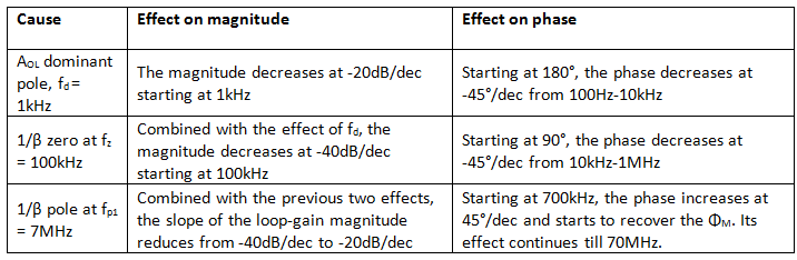
The zero causes the magnitude of 1/β to increase at 20dB/decade and intersect the AOL curve at a 40dB/decade rate of closure (ROC), resulting in potential instability. The dominant AOL pole at 1kHz results in a 90° phase shift in the loop gain. The zero frequency, fz, at 100kHz adds another 90° phase shift. Its effect is complete by 1MHz. Since the loop-gain crossover occurs at only 10MHz, the total phase shift from fd and fz will be 180°, resulting in ΦM = 0° and indicating that the TIA circuit is unstable.
 Figure 5 Simulation Circuit Including a 10pF Input Capacitor
 When Including the Effects of Input Capacitance") Figure 6 Simulated Loop Gain, aOL And (1/Β) When Including the Effects of Input Capacitance
Figure 6 Simulated Loop Gain, aOL And (1/Β) When Including the Effects of Input CapacitanceEffect of Feedback Capacitance (CF)
To recover the phase loss due to fz, insert a pole, fp1, into the 1/β response by adding capacitor CF in parallel with RF. fp1 is located at 1/(2πRFCF). To get a maximally flat, closed-loop Butterworth response (ΦM = 64°), calculate CF using Equation Figure 1:
") Figure 7 (1)
Figure 7 (1)where f-3dB is the closed-loop bandwidth shown in Equation Figure 1:
") Figure 8 (2)
Figure 8 (2)The calculated CF = 0.14pF and f-3dB = 10MHz. fz is located at ≈7MHz. The feedback capacitor includes the parasitic capacitances from the printed circuit board and RF. In order to minimize CPCB, remove the ground and power planes beneath the feedback trace between the amplifier’s inverting input and output pin. Using resistors with small form factors, such as 0201 and 0402 reduces parasitic capacitance caused by the feedback components. Figure 9 and Figure 10 show the circuit and resulting frequency response.
 Figure 9 Simulation Circuit, Including
a 0.14pF Feedback Capacitor
Figure 9 Simulation Circuit, Including
a 0.14pF Feedback Capacitor Figure 10 Simulated Loop Gain, aOL And 1/Β When Including the Effects of Input and Feedback Capacitance
Using Bode-plot theory, Table 2 summarizes the points of inflection in the loop-gain response.
|
The 1/β curve reaches a maximum value of 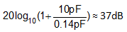 . For a Butterworth response, 1/β intersects AOL near its maximum value at a frequency
 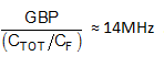 . fd and fz create a total phase shift of 180°. The phase reclaimed by fp1 is
 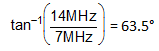 , which is very close to the simulated 65°.
When designing a TIA, you must know the photodiode’s capacitance, as this is usually fixed by the application. Given the photodiode capacitance, the next step is to select the correct amplifier for the application.
Choosing the right amplifier requires an understanding of the relationship between an amplifier’s GBP, the desired transimpedance gain and closed-loop bandwidth, and the input and feedback capacitances. You can find an Excel calculator incorporating the equations and theory described in this post here. If you are designing a TIA, be sure to check the calculator out. It will save you a lot of time and manual calculations.
Additional Resources
- Download the application report, “Transimpedance Considerations for High-Speed Amplifiers,” for a quantitative derivation of Equations Figure 1 and Figure 1 in this post.
- Get online support in the TI E2E™ Community Amplifier forums.
- Browse more than 40 training videos on op-amp topics like noise, bandwidth and stability.
- Learn more about selecting the correct amplifier in the application note, “Transimpedance Amplifiers (TIA): Choosing the Best Amplifier for the Job.”
- Search TI high-speed op amps and find technical resources.