SSZTBG0 April 2016 TL431 , UCC28911
For a bias power supply with a power level less than 10W, the biggest consideration about the design is its efficiency and its cost. In this post, I’ll compare two control schemes – primary-side regulation (PSR) and secondary-side regulation (SSR) – and offer some suggestions for how to get a more efficient and cost-competitive design.
The classic flyback topology shown in Figure 1 is still the most popular for power levels less than 10W, not only because its few external components can help you get a very competitive bill-of-materials (BOM) cost, but also because a flyback topology can easily realize multiple outputs, which is the key specification for a bias power-supply design.
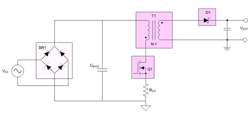 Figure 1 Classic Flyback
Topology
Figure 1 Classic Flyback
TopologySecondary-side Regulation
Figure 2 shows a typical SSR control block diagram. In order to stabilize the output voltage, the feedback from the output voltage is needed. For safety, isolated power supplies require non-galvanic feedback; the output must be electrically isolated from the AC input. Traditionally, an optocoupler transistor provides this isolation. Compared to the classic flyback topology, the key difference is adding an optocoupler such as the TI TL431, along with several resistors and capacitors, to constitute the feedback loop and error-amplifier-compensated circuit.
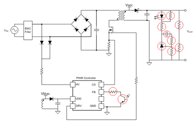 Figure 2 Typical SSR Flyback Block Diagram with Single Output
With optocoupler feedback, it is possible to choose which output to regulate, or to weight the impact each output has on loop demand by connecting a sense chain from each output, as shown in Figure 3. So you can easily get load regulation within ±1% if you used the SSR control law.
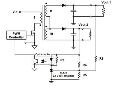 Figure 3 SSR Block Diagram with Multiple Outputs
Primary-side Regulation
Compared to an SSR topology, the PSR control method eliminates the optocoupler and compensated components (as shown in Figure 4). The magnetic field in the transformer provides the feedback. Although resistors and capacitors are pretty cheap (but error amplifier and optocoupler cost are not insignificant), this method does save cost and printed circuit board (PCB) area. The optocoupler’s aging characteristics will reduce the reliability of the design, so fewer components can increase mean time between failures (MTBF).
In the other hand, PSR controllers are typically internally compensated, which can save time and effort for control-loop design. For applications with high surge or isolation voltage requirements, reducing the number of components crossing the isolation barrier reduces the number of areas that could potentially break down.
For a PSR controller’s crossing regulation, the most heavily loaded output sets the loop demand. The other outputs may be poorly regulated if lightly loaded. And because most PSR controllers use “knee point sampling” for feedback, the controller only operates in discontinuous conduction mode (DCM). The output voltage ripple will be higher than in continuous conduction mode (CCM).
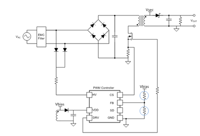 Figure 4 PSR Block Diagram with Single Output
Figure 5 compares some key features between PSR and SSR control law.
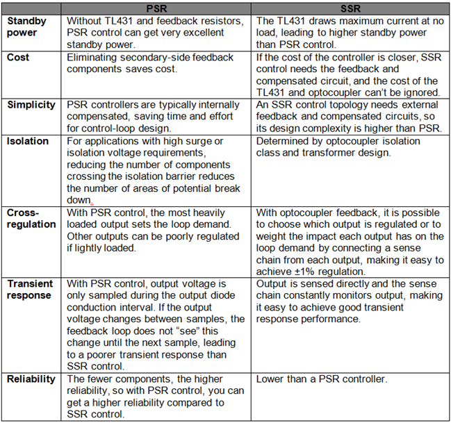 Figure 5 Quick Comparison of Key
Features between PSR and SSR Control
Figure 5 Quick Comparison of Key
Features between PSR and SSR ControlNew Reference Design
The Universal Input, 10-W, High Efficiency, Low-Cost Power Supply with Isolated Multiple Inputs reference design is designed for bias power of appliances, operating in constant-voltage (CV) and constant-current (CC) flyback using TI’s UCC28911 controller. That high-voltage switcher integrates a high-voltage power FET plus a controller that uses PSR, supporting magnetically sensed output voltage regulation via the transformer bias winding. The sensing eliminates the need for a secondary-side reference, error amplifier and optical isolator for output-voltage regulation. The magnetic sampling scheme allows operation only in DCM, so the device is not allowed to turn on the power FET if it doesn’t sense a zero crossing detector (ZCD) event such as when the auxiliary winding voltage crosses zero from high to low after transformer demagnetization is complete. The modulator adjusts both frequency and peak current in different load regions to maximize efficiency throughout the operating range. Smart management of the control logic power consumption and the high-voltage current source, used for startup that is off during operation and has very low leakage current, allow you to design converters with very low standby input power.
The key highlights of this reference design are:
- More than 75% low load efficiency under 10% load
- Less than 30-mW standby power under 90-V input
- Valley Switching and Frequency Dithering to Ease EMI Compliance
Figure 6 and Figure 7 show a simple schematic and efficiency curves, respectively.
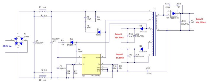 Figure 6 Multiple-output Flyback Converter Based on the UCC28911
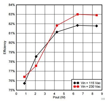 Figure 7 Efficiency Curves at 230VAC And 115VAC Inputs
Summary
The flyback converter is the most popular topology for low-power isolated power supplies. While easy to realize multiple outputs with low cost, this topology still has poor transformer utilization and high AC resistance losses.
If you want to achieve good transient response performance and need a high-accuracy output, the SSR control topology is more suitable. If the design is very sensitive to cost and standby power consumption, choose the PSR controller.
Additional Resources
- Learn more about the UCC28911 flyback switcher.
- Read “Designing multiple output converters with primary side sensing” blog post on Power House.
- Visit “Measuring PSRR in an ADC” blog post.