SSZTBT1 december 2015 LM3481
It can be quite daunting for a design engineer to work with applications that require a high voltage from a low voltage. It doesn’t have to be that way, however, if you have a basic understanding of magnetics and power architectures.
Some of the more common applications requiring a high voltage from a low voltage include cellphone chargers; standby power supplies; and low-cost multiple power supplies for consumer applications such as TVs, monitors, lasers, copiers and isolated gate drivers.
The simplest solution is to use a flyback converter, which uses galvanic isolation between the input and output and can convert either AC/DC or DC/DC. The flyback is basically a buck-boost converter where the inductor is set up to form a transformer. Within the design, the transformer is used to multiply the voltage but is also useful as it adds the benefit to the design of isolation. For example, when surge suppression parts are used at the input and the output, with the whole line isolation, it helps in the continuous filtering of power line noises in all modes or protects sensitive circuitry or even humans from shock when touching equipment.
When a flyback converter’s primary switch is closed, the transformer’s primary side is connected to the input voltage source. The energy is stored in the transformer as the current and magnetic flux increases. When the primary switch is open, the energy in the transformer decays and the transformer’s secondary-side voltage becomes positive, allowing current to flow from the transformer through the forward-biased diode. The energy recharges the output capacitor, which supplies the point of load.
This operation allows the converter to generate larger voltage outputs than the voltage source without a lot of additional circuitry, components or complexity. The turns ratio of the transformer and the duty cycle dictate the amount of output voltage. Flyback converters can be either voltage mode or current mode, though current mode is more common because it is easier to stabilize. Both architectures need to be able to measure the output voltage without breaking the galvanic isolation (if galvanic isolation is not required, a simple voltage divider works); there are several methods for achieving this. A common method is to use an optocoupler on the secondary side. Another method often used in low-cost applications is to use the primary-side voltage, either by monitoring directly or with a second winding.
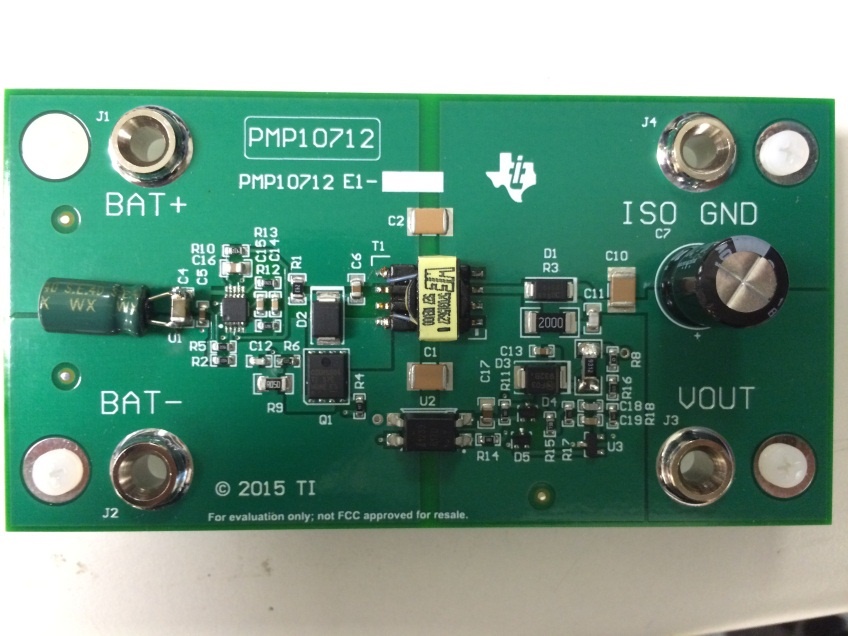
To demonstrate flyback-converter operation and support our customers’ designs, we built the TI Designs Low VIN, Small Form Factor Flyback Reference Design for High Voltage Laser Flash Drives (Figure 1). This design is a 1.2W isolated flyback design that supports very low VIN of 3.3V to 6V and is capable of delivering 10mA at 120V output. The design uses the LM3481 boost controller integrated circuit (IC), which works on current-mode operation and is synchronizable to any frequency between 100 KHz and 1 MHz. This design was built on a two-layer board and is a simple, low-bill-of-materials, low-cost design providing an isolated output. As it is often the most expensive part of the overall solution, developing the design on a two-layer printed circuit board (PCB) helps reduce system-implementation challenges in consumer-based applications.
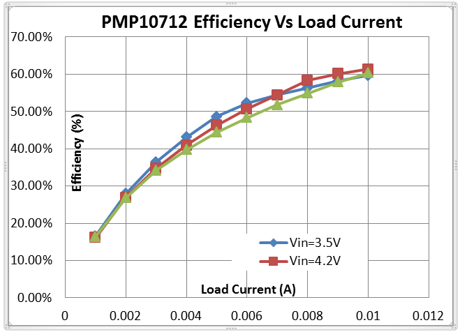
The reference design uses devices that can support input voltages from 3V to 42V. By tailoring the design, it is possible to increase both the output voltage and the power rating. See Figure 2 for overall system efficiency.
 Figure 2 Efficiency Using the LM3481 Boost Controller
The LM3481 boost controller is well-suited to flyback design as it is highly flexible, easy to design and offers a small solution size.
Additional Resources
-
Download the TI Design Flyback reference design Low Vin, Small Form Factor Flyback Reference Design for High Voltage Laser Flash Drive.
-
Consider the LM3481 boost controller for your next design.
