SSZTCA0 August 2015 LMG5200
Gallium nitride (GaN) transistors switch fast! In a previous post, I examined the LMG5200 half-bridge GaN driver, and showed that it is capable of a switching rise time of 600 ps or less. On the bench, I measured a switch-node dv/dt of 40-V per nanosecond! That’s about 30 times higher than the typical DC/DC converters I work with, and while this can help reduce switching losses, it does make the challenge of meeting electromagnetic compliance (EMC) much harder. Why? Because the rate of change of voltage and current activates parasitic circuit elements to produce noise sources that radiate and conduct noise.
Experienced power-supply designers know that they must carefully consider component selection, component placement and circuit-board trace routing when minimizing switch-mode power supply (SMPS) electromagnetic interference (EMI). With the introduction of wide-bandgap transistors and their picosecond switching speeds, the challenge of passing agency requirements (such as, those from the FCC and CISPR) for EMC just got harder – a lot harder. Parasitic circuit elements and PCB antenna structures that were benign with slower MOSFET transistors can be 10-to-100 times more active when replaced with GaN transistors.
The good news is that there are low-cost ways to help visualize and isolate problems on the bench before heading to an EMC certification lab. Ultimately, these tools will help accelerate a GaN design to EMC. In this post, I’ll examine some of the equipment that you can use to qualify the problem; later, in a follow-up post, I’ll qualify a solution.
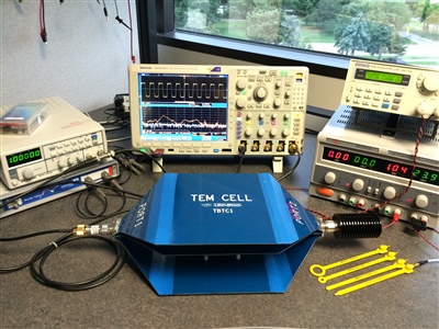
The first piece of equipment necessary for measuring EMI is a spectrum analyzer (SA). Acceptable performance can be found for around $1,500. On my bench I’m using a MDO4104-6 mixed domain (Time and Spectrum Domain) oscilloscope with a SA input good to 6 GHz. I also make use of E-field and H-field probes to localize problem areas on the board – Figure 1 shows both the MDO4104-6 and field probes.
When picking H-field and E-field probe shielding, resolution and sensitivity are important. Years ago, Bruce Carsten developed an “EMI sniffer” probe that was able to localize EMI problems at the PCB trace level – spatial resolution was about 1mm. The probes like those on my on my bench can be purchased for around $300. Figure 1 also shows a transverse electromagnetic open (TEM) cell that I use to quickly determine how good (or bad) a SMPS design is. The TEM is a versatile, low cost and (in my opinion) necessary piece of equipment for pre-compliance-radiated emission testing. See this excellent article for details on how a TEM works and how to build one.
The TEM is a two-port stripeline device where the center plate, called the septum, is sandwiched between two ground planes (open in this case, so not perfect) and designed for 50Ω. Figure 2 shows the connection between the device under test (DUT) and the SA. Agency-standard units for EMI are in dBµV for conducted emissions and dBµV/meter for radiated emissions. Note that when measuring radiated emissions with the setup shown in Figure 2, the SA will display emissions in dBµV. The procedure and mathematics to convert this dBµV measurement into an effective reading in dBµV/meters is complicated and even when done correctly (in all three ordinations), the correlation with a certified lab is only good to about 6dB. For this reason, I prefer to use the TEM for “qualitative measurements.”
For example, given the geometry of the TEM cell, if the SA is displaying spurs greater than 40dBµV, the possibility of failing radiated emissions in a certified EMC chamber exists. Also PCB board resonant peaking can be especially problematic and can make an otherwise good design fail emissions.
 Figure 1 TEM Cell Measurement Setup
with the LMG5200
Converting 24 V to 12 V at 1 MHz and 24 W
 Figure 2 Configuring a DUT for Emission
Testing
Figure 2 Configuring a DUT for Emission
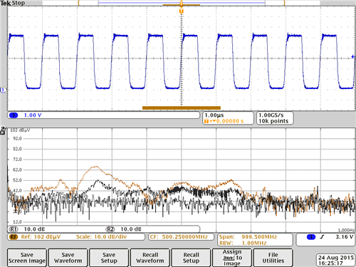
TestingFigure 3 shows what the SA sees between 500 kHz and 1 GHz with the LMG5200 EVM converting 24 V to 12 V at no load and at 24 W. The lower black trace is representative of the ambient noise. The upper black trace is the LMG5200 switching, but without a load, and the brown trace is with a 24W DC load – the fact that there is relatively little difference between the upper black trace and the brown trace suggests a pre-existing condition that I was able to isolate to the input caps using my field probes. The 250-MHz resonance has a peak of over 62 dBµV - about 100 times greater than what I would typically accept before going to a compliance lab.
 Figure 3 LMG5200
Operating at 1 MHz – Brown 24 W Load, Upper Black No-load, Lower Black
Trace Ambient Noise
Figure 3 LMG5200
Operating at 1 MHz – Brown 24 W Load, Upper Black No-load, Lower Black
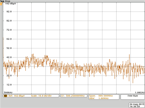
Trace Ambient NoiseFor comparison purposes Figure 4 illustrates an EMC-optimized, DC/DC converter operating at twice the frequency (2 MHz) converting 15 V to 7.5 V at 2 A. The rise time of the switch node is about 10ns or about 10 times slower than the LMG5200. With peaks of 42 dBµV, the emissions are 100 times less than the case above.
 Figure 4 15 V to 7.5 V (15 W, 50% Duty)
DC/DC Converter Optimized for EMI Operating at 2 MHz the Rise Time of the Switch
Node Is Only 10 ns Compared With 600 ps.
Figure 4 15 V to 7.5 V (15 W, 50% Duty)
DC/DC Converter Optimized for EMI Operating at 2 MHz the Rise Time of the Switch
Node Is Only 10 ns Compared With 600 ps.Because wide-bandgap semiconductors have much faster switching edges, parasitic, PCB, and component impedances will become increasingly problematic. To comprehend and quantify this effect, RF test equipment and know how will be necessary. Tools like TEM cells and field probes are effective and essential for anyone working with this technology because you can use them to empirically isolate EMI for the purpose of pre-compliance, radiated emission testing. In my next post, I’ll look at some soft tools that you can use to virtually analyze PCB and component electromagnetic field behavior and address them at the source.