SSZTCC7 august 2015 TPS65911 , TPS65912
Power has always been a challenge for most designers to route on the board. Designers face challenges around power density, component placement, selecting the number of printed circuit board (PCB) layers and cross-coupling between signals. With the complex integration of many power sources into a single package, PCB design can be even more difficult. But you can mitigate the challenges by following a few rules.
Before considering PCB layout, you must first address PCB buildup. You will have to decide which components you need and where to place them, as there are several different ways. Depending on the application, you may need to adjust each PCB accordingly and/or make a variety of trade-offs.
Irrespective of application, all designs follow a few basic rules for component placement. A power management integrated circuit (PMIC) usually includes the integration of several power sources, such as buck converters, boost converters, linear dropout regulators (LDOs), reference voltages, clocks and general-purpose inputs/outputs (GPIOs). Each power source will require components such as capacitors, inductors and resistors. It is very important to start placing components at the input pins of the PMICs. The input capacitors for the PMIC must be very close to the PMIC, and on the same layer of the board. The output pins of the PMIC take precedence after the input capacitors.
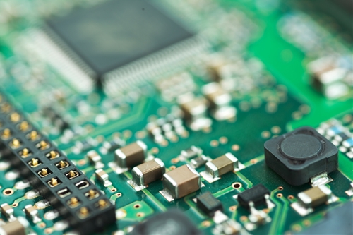
While component placing for the PMIC you will have to consider where to place output pins based on the power source. First, place the components related to the reference block after the input capacitors. Second, place the inductors for the buck converters on the same layer as the PMIC after the reference-block components. Third, place the buck-converter output capacitors after the inductor. If that’s not possible, place these components right beneath the PMIC on the bottom layer, connected with several vias per component. (There is a slight difference in the placement scheme for boost converters; precedence is given to the inductor.) The last components to consider are the LDOs. Figure 1 shows an example of an effective placement scheme for PMICs.
 Figure 1 Passive Placements around
PMIC
Figure 1 Passive Placements around
PMICIf you follow these ground rules for component placement, then your layout decisions for power management ICs will become much easier. By placing component this way you will have enough space on board to route the traces. It will give you more room for necessary adjustments for signal traces between components.
Additional Resources
- Check out layout examples for the TPS65911 and the TPS65912
- View TI’s entire PMIC portfolio: www.ti.com/pmic