SSZTCM5 june 2015 LM5119
To combat ever-stringent power requirements from the industrial and automotive industries, multiphase designs are a popular choice for engineers these days. For current requirements over 25A, more designers are opting for multi-phase approaches because of the key benefits they provide. Multiple phases provide lower output-ripple voltages when compared to single-phase designs, as well as better transient performances and better thermal performance, leading to higher efficiencies overall.
To achieve these key benefits in a synchronous buck converter, designers must interleave the phases. Although many integrated circuits (ICs) exist that interleave dual phases, the challenge arises when more than two phases are required. In this PMP10979 reference design, two dual-phase synchronous buck controllers, are connected in parallel to achieve a four phase design. Figure 1 and Figure 2 showcase how the PMP10979 is capable of providing 13.5V at 95A (1282W) with an input voltage of 24V.
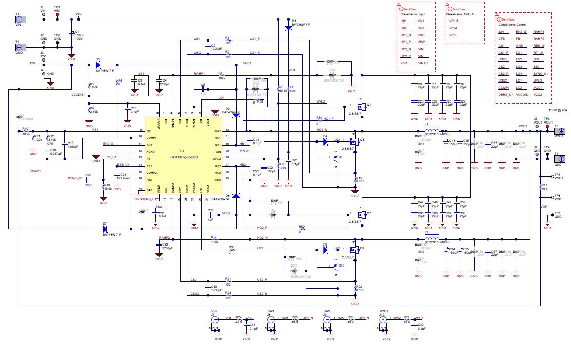 Figure 1 Phases 1 and 2 of
PMP10979
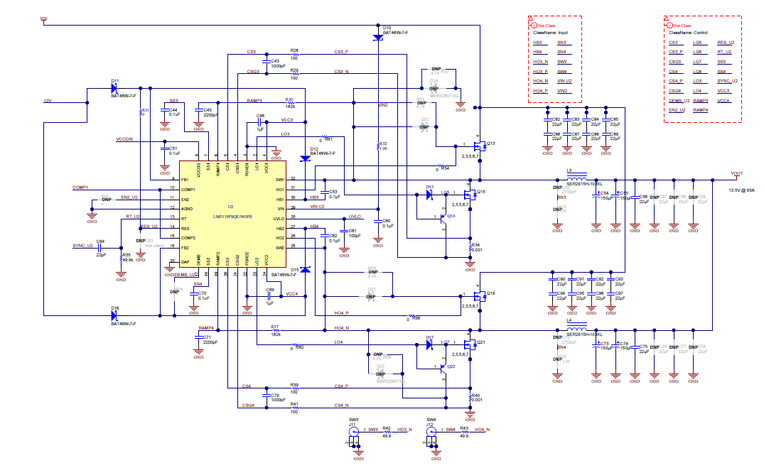 Figure 2 Phase 3 and 4 of PMP10979
 In order to maximize the benefits of this four-phase design (decreasing input/output ripple current, leading to a decrease in the stress on the inductor/field effect transistor [FET]), you need to run the phases 90 degrees apart. The internal oscillator of the LM5119 buck controller ensures that every dual- phase design runs 180 degrees out of phase. To ensure a 90-degree phase shift between the four phases, a synchronous external clock signal must be provided to both ICs. This can be achieved easily by using a 555 timer and inverter, as shown in Figure 3. The timer will output a square wave with a 50% duty cycle at twice the switching frequency of one of the LM5119 controllers, as well as an inverter. The output of the inverter will be routed to the other IC.
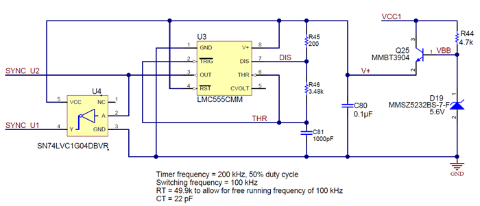 Figure 3 External clock circuitry for
90-degree phase shifting
Figure 3 External clock circuitry for
90-degree phase shiftingThis ensures that with every rising edge of the square wave, an IC triggers a switching cycle resulting in a phase sequence of phase 1, phase 3, phase 2, and phase 4, all shifted by 90 degrees. If you adjust the input voltage of the design to produce a 50% duty cycle, the 90-degree phase shift becomes apparent, as Figure 4 shows.
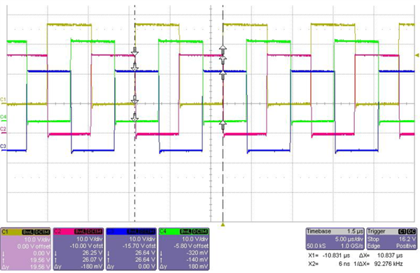 Figure 4 Switch node waveforms for 4
phases showing 90 degree phase shifting
Figure 4 Switch node waveforms for 4
phases showing 90 degree phase shiftingKeeping the switching frequency for each phase lower than 200 kHz will ensure that switching losses are minimized in the high-side FET. Also, splitting the current into four phases reduces conduction losses in the low-side FET. Thermal performance is further improved because the total dissipation of power is now shared among many smaller components, as highlighted in Figure 5.
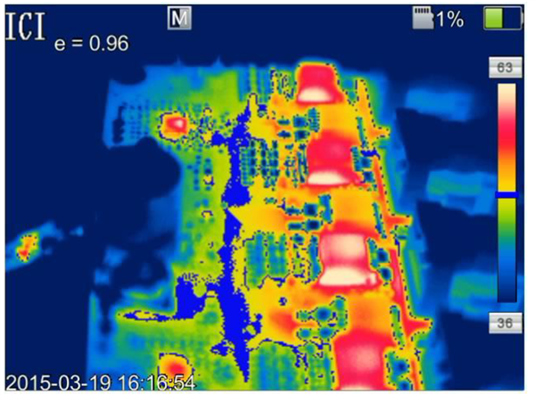 Figure 5 Thermal performance at 1,280W
output (PMP10979)
Figure 5 Thermal performance at 1,280W
output (PMP10979)For more Power Tips like these, visit our Power Tips blog series.