SSZTCP0 may 2015 CSD18535KCS , CSD18536KCS
Welcome back, fellow FET enthusiasts to part three of the "Understanding MOSFET Data Sheets" blog series! Today I’ll be talking about MOSFET current ratings and how they’re not real. Ok, so maybe a better way to put it is just that they are not measured the way that parameters like RDS(ON) and gate charge are determined, but rather, they are calculated, and can be arrived at in many different ways. Note that if you are more of a visual learner, you can watch the video "Understanding MOSFET data sheets - current ratings".
For instance the “package current rating” of the FET is for the most part, independent of ambient temperature, and is a function of the internal connections between the silicon die and the plastic package. Exceeding this value does not immediately guarantee that the FET will die, so much as prolonged use above this limit will begin to reduce the lifetime of the device. Failure mechanisms above this limit include but are not limited to wire fusion, thermal degradation of the molding compound, and issues cause by electromigration stresses.
Then there is what we consider the “silicon limit,” usually specified by holding the case temperature to 25˚C. This condition basically assumes an ideal heat sink, as only the junction to case thermal impedance is used to calculate the max power the device can handle (shown in equations Figure 1 and Figure 1 below). In other words, RθCase-to-Ambient is assumed to be zero, not a very practical condition in application, such that this current rating is best thought of as a figure of merit that accounts for both the RDS(ON) and thermal impedance of the device.
 Figure 1 (1)
 Figure 2 (2)
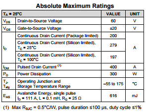
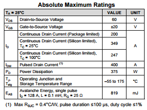
As an example, below in Figure 3a and 1b are the respective absolute maximum ratings tables appearing on the front page of the datasheet for the CSD18536KCS and the CSD18535KCS 60V TO-220 MOSFETs. Both of the devices are package limited to 200A, but because the CSD18536KCS has lower RDS(ON) and thermal impedance, it has a higher silicon limit of 349A, indicating that it should run cooler than the CSD18535KCS when handling the same amount of continuous current. We still would not recommend ever operating these devices over 200A for any long duration of time. In the FET world, that means any current pulse longer than 100ms, above which can basically be considered DC.
 Figure 3 A: CSD18535KCS Absolute Maximum Ratings
Table
 Figure 4 B: CSD18536KCS Absolute Maximum Ratings
Table
Figure 4 B: CSD18536KCS Absolute Maximum Ratings
TableSome QFN datasheets also include a third continuous current, which is calculated with the exact same methodology as the silicon limit, but as a function of the measured RθJA of the device as called out in a footnote below the table. Using RθJA instead (typically 40˚C/W for a standard SON5x6) to calculate the max power assumes that in application, a QFN can really only handle around about 3W of power. Therefore, this calculation yields a somewhat more practical DC current limit for a QFN device not exposed to any heat sink or other cooling mechanism.
In part four of “Understanding MOSFET data sheets,” I will provide a similar analysis for the pulsed current rating, IDM, and show how this ties in to the other parameters on the datasheet, including the SOA. In the meantime, watch a video "NexFET™:Lowest Rdson 80 and 100V TO-220 MOSFETs in the World" and consider one of TI’s NexFET power MOSFET products for your next design. And for more on FET thermal constraints and currents,