SSZTCX9 February 2024 UCC28910
One of the most common sources of power is offline, also known as the AC mains. With the increase of products aimed at integrating typical household features, there is greater demand for low-power offline converters that require less than 1W of output capability. For these applications, the most critical design aspects are efficiency, integration, and low cost.
When deciding on a topology, the flyback is typically the first choice for any low-power offline converter. Where isolation is not required, however, this may not be the best approach. Let’s say that the end equipment is a smart light switch that users control through a smartphone app. In this case, the user will never be in contact with exposed voltages during operation, so isolation is not required.
For an offline supply, the flyback topology is a reasonable solution, as it has a low bill-of-materials (BOM) count with only a few power-stage components, and the transformer can be designed in such a way to handle a wide input voltage range. But, what if the end application for a design doesn’t need isolation? If this is the case, a designer would be tempted to still use a flyback considering that the input is offline. A controller with an integrated field-effect transistor (FET) and primary-side regulation would create a small flyback solution.
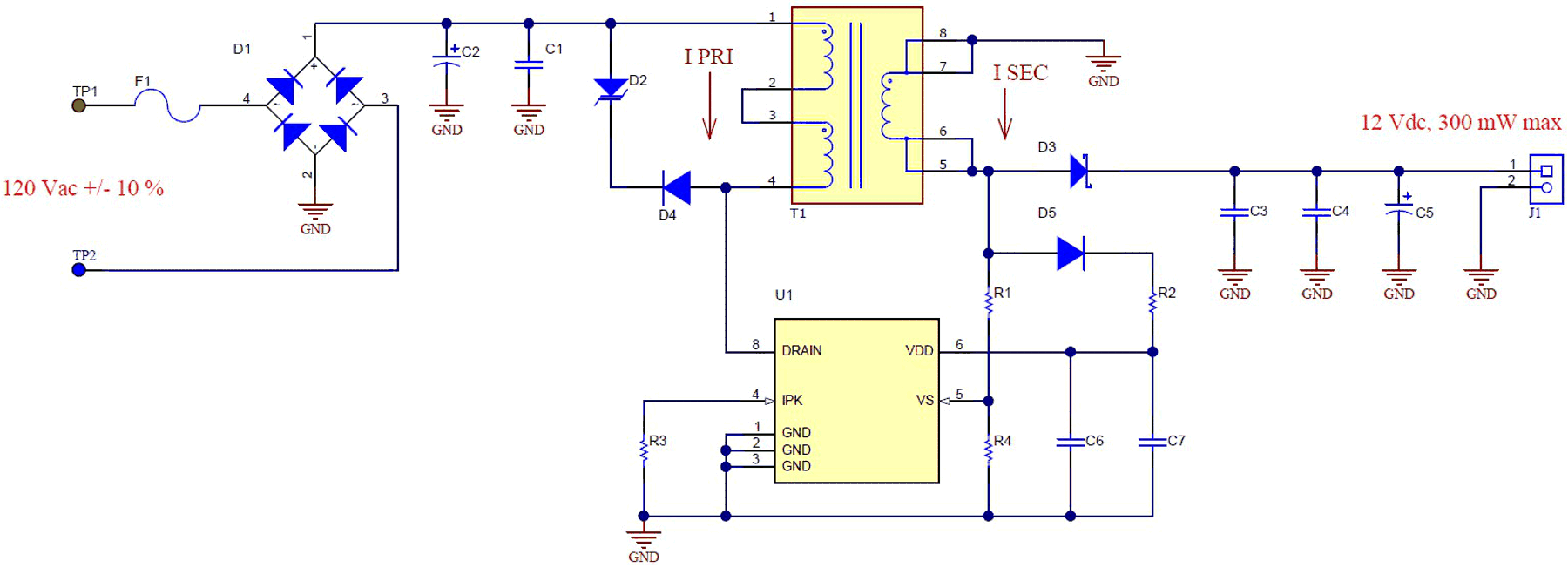
Figure 1 shows an example schematic of a nonisolated flyback that uses a UCC28910 flyback switcher with primary-side regulation. While this is a viable option, an offline upside-down buck topology will provide higher efficiency compared to a flyback, with a lower BOM count. In this Power Tip, I will be exploring the benefits of an upside-down buck for a low-power AC/DC conversion.
 Figure 1 This non-isolated flyback
design using the UCC28910 flyback switcher converts AC to DC, but an offline
upside-down buck topology can do the job more efficiently.
Figure 1 This non-isolated flyback
design using the UCC28910 flyback switcher converts AC to DC, but an offline
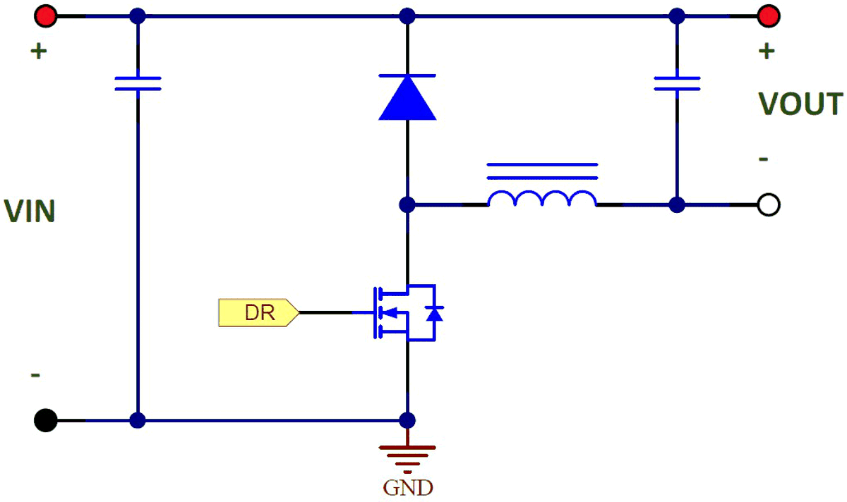
upside-down buck topology can do the job more efficiently.Figure 1 shows the power stage of an upside-down buck. Like a flyback, there are two switching components, one magnetic (a single power inductor instead of a transformer), and two capacitors. The upside-down buck topology, as the name suggests, is similar to a buck converter. The switches create a switching waveform between the input voltage and ground, which is then filtered out by an inductor-capacitor network. The difference is that the output voltage is regulated as potential below the input voltage. Even though the output is “floating” below the input voltage, it can still power downstream electronics normally.
 Figure 2 A simplified schematic of an
upside-down buck power stage.
Figure 2 A simplified schematic of an
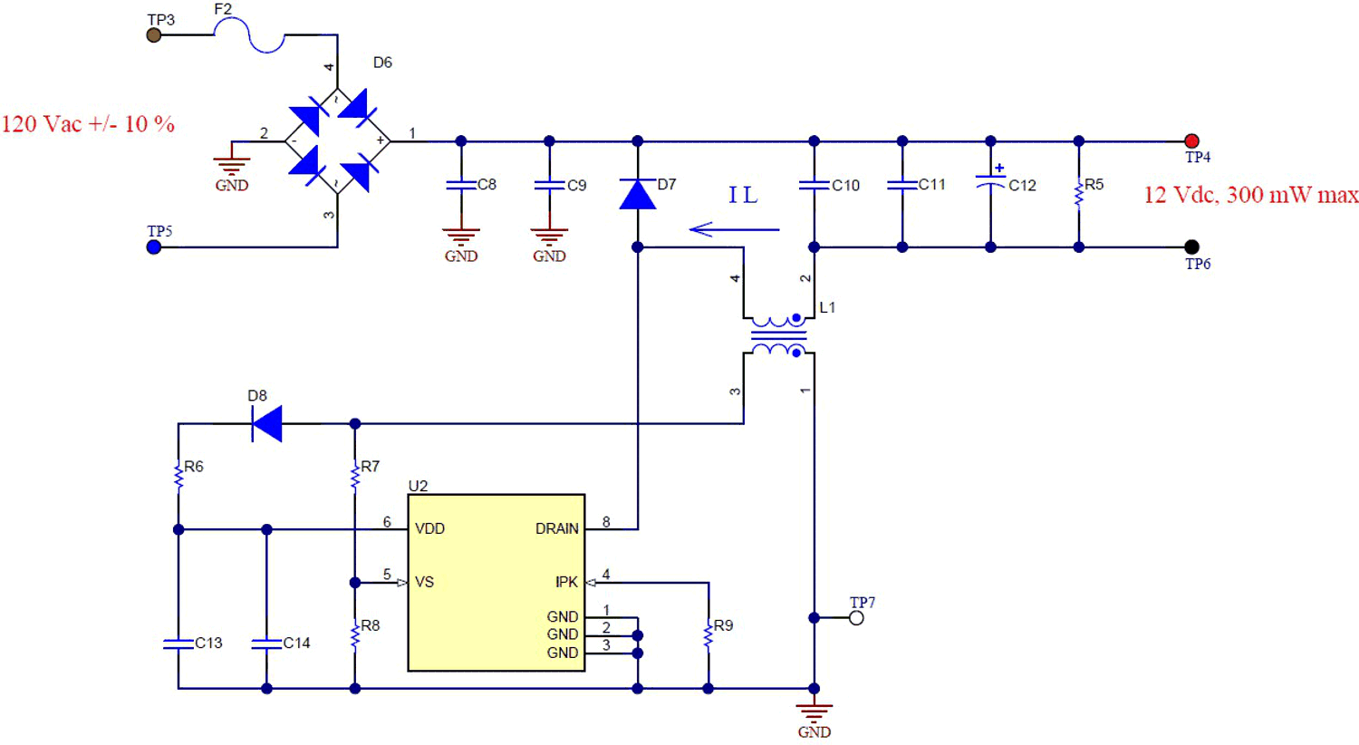
upside-down buck power stage.Having the FET on the low side means it can be driven directly from a flyback controller. Figure 3 shows an upside-down buck that uses the UCC28910 flyback switcher. A one-to-one coupled inductor functions as the magnetic switching component. The primary winding is acting as the inductor for the power stage. The secondary winding provides timing and output voltage regulation information to the controller and charges the controller’s local bias supply (VDD) capacitors.
 Figure 3 An example upside-down buck
design using the UCC28910 flyback switcher.
Figure 3 An example upside-down buck
design using the UCC28910 flyback switcher.One drawback of the flyback topology is how energy transfers across the transformer. This topology stores energy in the air gap during the FET’s on-time and transfers it to the secondary during the FET’s off-time. An actual transformer will have some leakage inductance on the primary side. When energy transfers to the secondary side, what remains is stored in the leakage inductance. This energy is not usable, and requires dissipation using either a Zener diode or a resistor-capacitor network.
In a buck topology, the leakage energy is delivered to the output during the FET’s off time through diode D7. This reduces the component count and improves efficiency.
Another difference is the design and conduction losses for each magnetic. Because an upside-down buck only has one winding to transfer power, all of the current for power delivery goes through it, which provides good copper utilization. A flyback does not have as good copper utilization. When the FET is on, current conducts through the primary winding but not in the secondary. When the FET turns off, current flows on the secondary winding and not in the primary. Thus, more energy is stored in the transformer and uses more copper in the flyback design to deliver the same amount of output power.
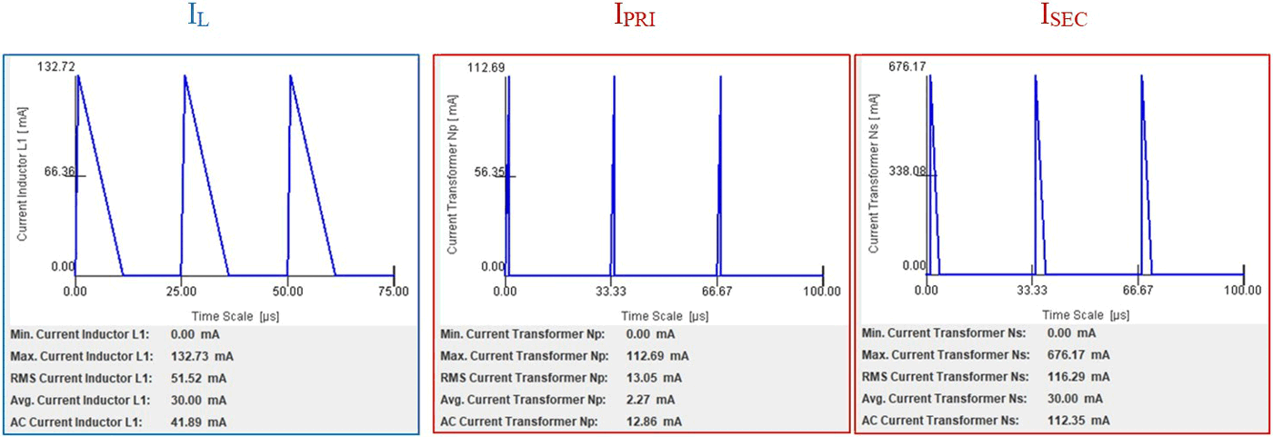
Figure 4 compares the current waveforms for an inductor of a buck and the primary and secondary windings of a flyback transformer with the same input and output specifications. The buck inductor waveform is in the single blue box on the left, and the primary and secondary windings of the flyback are in the two red boxes on the right.
For each waveform, the conduction loss is calculated as the root-mean-square current squared multiplied by the winding’s resistance. Because the buck only has one winding, the total conduction loss in the magnetic is the loss from the one winding. The total conduction loss for the flyback, however, is the sum of the losses from the primary and secondary windings. Additionally, the magnetic will be physically larger in a flyback compared to an upside-down buck design at a similar power level. The energy storage for either component is equal to ½ L × IPK2.
For the waveforms shown in Figure 4, I calculated that the upside-down buck would only need to store one quarter of the power that the flyback would need to store. As a result, an upside-down buck design would have a much smaller footprint compared to an equally powered flyback design.
 Figure 4 A comparison of current
waveforms in buck vs. flyback topologies.
Figure 4 A comparison of current
waveforms in buck vs. flyback topologies.When isolation is not required, the flyback topology isn’t always the best solution for a low-power offline application. An upside-down buck can offer higher efficiencies with a lower BOM cost because you can use a potentially smaller transformer/inductor. For a power electronics designer, it is important to consider all possible topology solutions to determine the best fit for the given specifications.
Related articles:
- Power Tips #76: Flyback converter design considerations
- Power Tips #91: How to improve flyback efficiency with a nondissipative clamp
- Creating an isolated power supply creates many challenges
- Isolated power conversion: making the case for secondary-side control
- Build your own oscilloscope probes for power measurements (part 1)
- Build your own oscilloscope probes for power measurements (part 2)
Previously published on EDN.com.