SSZTCZ1 August 2023 TMS320F28P650DK
Power electronics designers are striving to increase power efficiency and power density in industrial and automotive designs ranging from multiaxis drives to solar energy storage to electric vehicle (EV) charging stations and EV onboard chargers.
One of the primary design challenges is achieving better real-time control performance while reducing system costs. A common approach to address this challenge is to use highly integrated microcontrollers (MCUs) with analog and control peripherals capable of ultra-low-latency control-loop processing.
Real-time control performance: it’s all about the latency
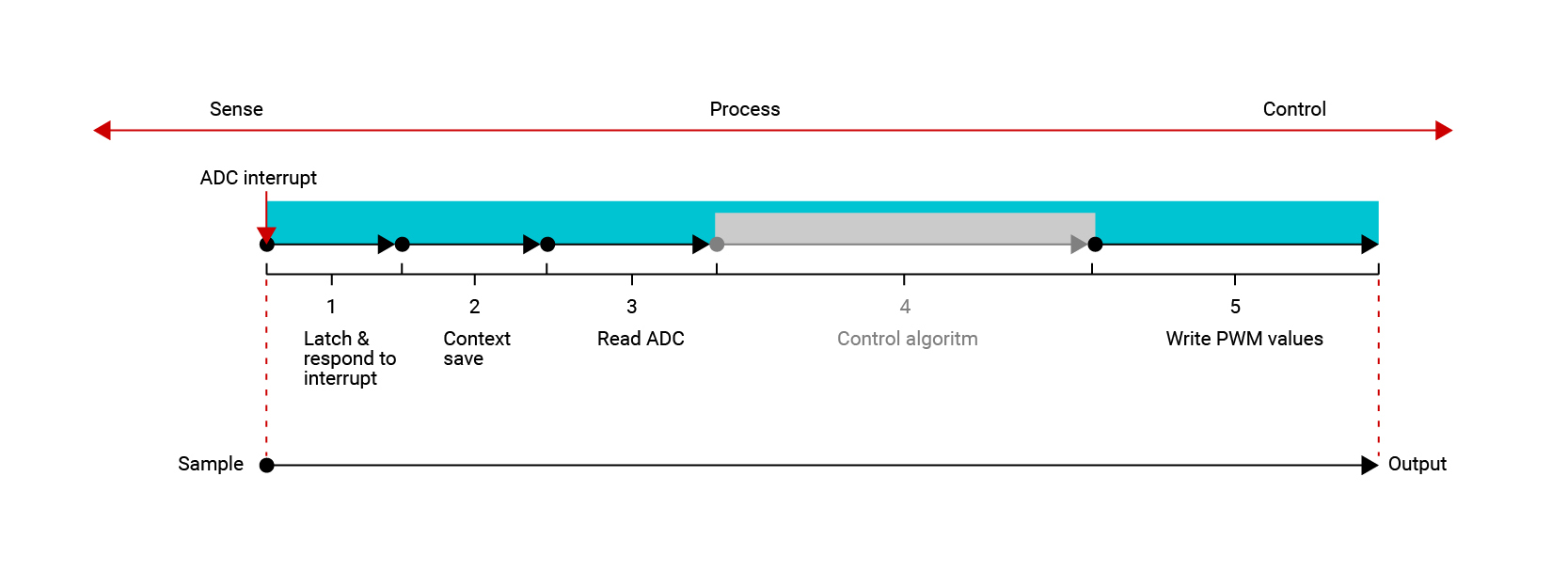
Before diving into some examples, let’s look at latency at a high level. In multiaxis drives, robotics, solar inverters with energy storage systems, EV charging stations and EVs themselves, control performance is directly related to how fast an MCU can sample, process and control signals. Figure 1 shows the real-time signal chain and signal latency from when the analog-to-digital converter (ADC) measures the signals to when the CPU processes the information and, ultimately, when the pulse-width modulator (PWM) controls the power stage. You want this number to be as small as possible in order to achieve ultra-low-latency control-loop processing.
 Figure 1 The concept of real-time
performance and latency
Figure 1 The concept of real-time
performance and latencyFor digital power, achieving higher power density can mean increasing the switching frequencies of a DC/DC stage from 50 kHz to 100 kHz, 500 kHz and even more. If you use an MCU running at 100 MHz with a regulation loop synchronized to the PWM frequency, at 10 kHz you have 10,000 CPU cycles available between each PWM interrupt, dropping to 1,000 cycles at 100 kHz. As the frequency increases, the time available to sense process control decreases, and you need to have your MCU architecture optimized to save every cycle possible in the real-time signal chain.
Enabling next-generation power supplies in solar inverter energy storage systems
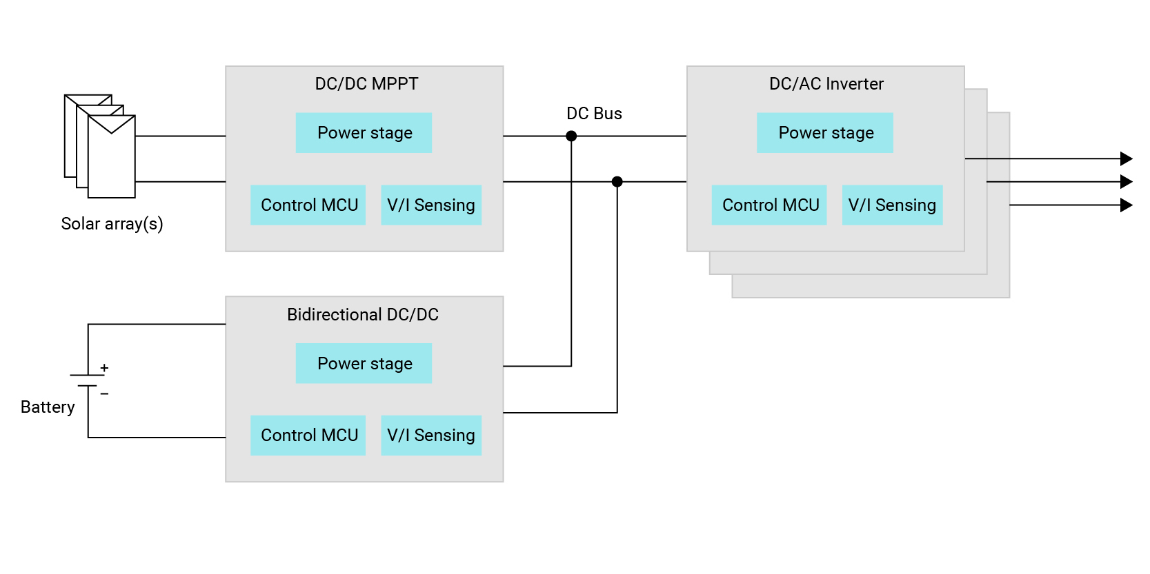
The solar inverter market is evolving with the integration of energy storage systems (hybrid inverters), as shown in Figure 2, which bring the challenge of bidirectional energy flow control. A single-chip architecture requires an MCU with a large number of high-resolution PWM channels and additional high-bandwidth ADC inputs, such as the TMS320F28P650DK C2000™ 32-bit MCU.
 Figure 2 A solar inverter architecture
with energy storage integrated
Figure 2 A solar inverter architecture
with energy storage integratedTo meet growing demands for renewable energy across applications, solar inverters need higher power efficiency and improved total harmonic distortion performance. One approach is to move to newer multiphase, multilevel inverter power architectures that are typically implemented with a combination of complex power algorithms and additional external logic such as a complex programmable logic device or field-programmable gate array in order to turn power switches on and off with the right sequence and safely. This adds board space and system costs.
An MCU capable supporting onboard custom, minimum deadband and illegal combo logic (an MCU feature that prevents a destructive on/off sequence) across different PWM modules will help further simplify designs by giving designers an opportunity to reduce or even remove external logic, while reducing costs.
It’s also important to closely couple PWM units with integrated analog-like window comparators in order to protect power converters against overcurrent and overvoltage events. Depending on the power topology, you will need to pick an MCU with PWM units capable of implementing resonant-mode converter peak current and valley current-mode control.
Enabling easier and faster integration in EV onboard chargers
As the number of EVs increase across the world, designers need to find new solutions to further integrate and reduce costs for the onboard charger. A typical implementation consists of one MCU for the onboard charger power factor correction stage and another MCU for the onboard charger DC/DC stage, with isolation in between.
While implementing a single MCU may increase the isolation needed to send signals back to the MCU, the cost is offset by savings from a reduced number of components, including fewer Controller Area Network transceivers, voltage regulators, power-management integrated circuits, operational amplifiers and isolation for the communication back to the host MCU.
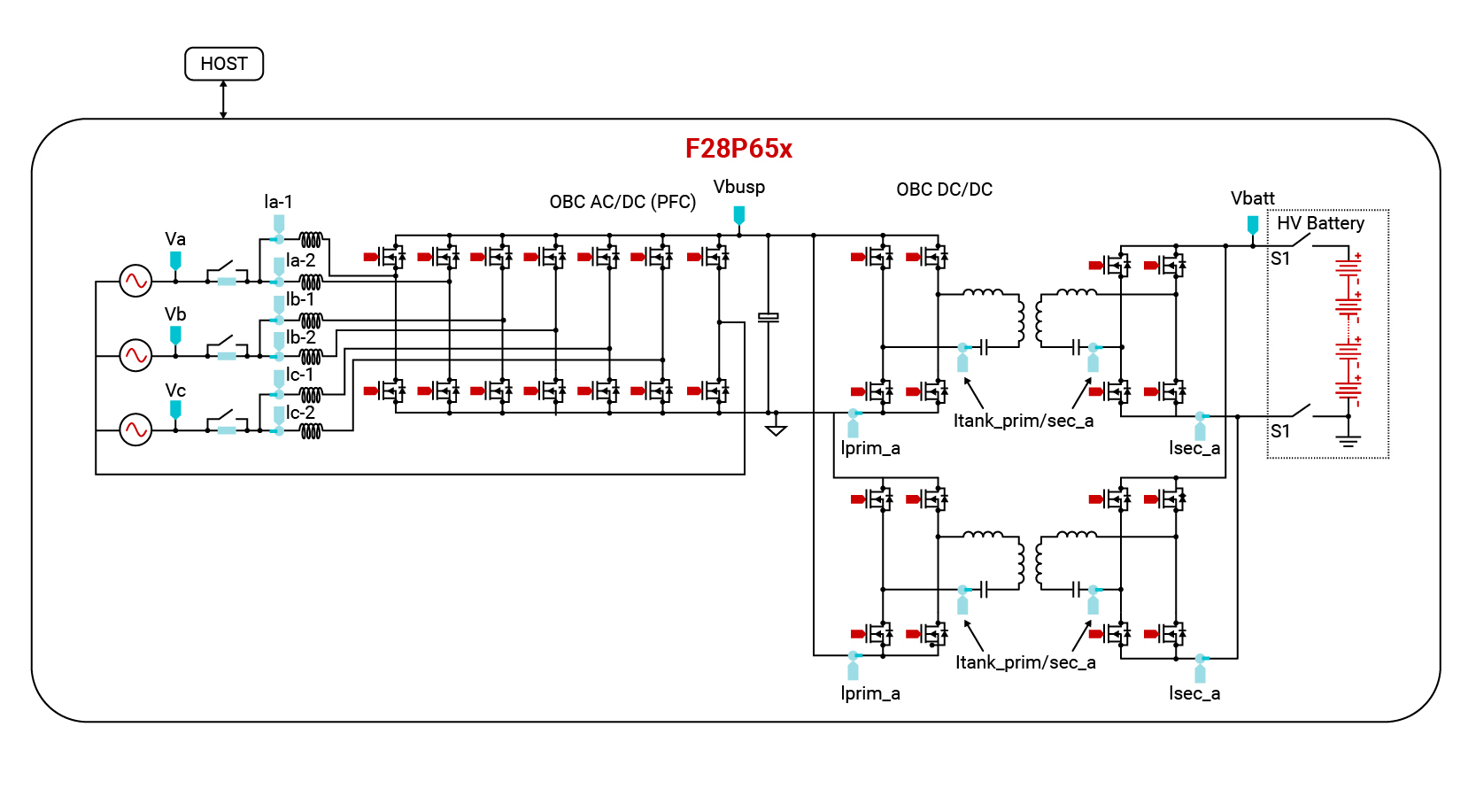
Figure 3 shows a single MCU controlling a three-phase onboard charger power-stage topology up to 22 kW. The PFC stage is a two-phase interleaved totem pole and the DC/DC stage is a dual capacitor-inductor-inductor-inductor-capacitor (CLLLC) that will reduce the transformer size and current rating of the field-effect transistor.
 Figure 3 A three-phase EV onboard
charger (PFC plus DC/DC) controlled by a single MCU
Figure 3 A three-phase EV onboard
charger (PFC plus DC/DC) controlled by a single MCUAfter addressing the minimum required MCU hardware resources (PWMs, ADCs, comparators), you will also want to look for more software integration while reducing CPU overhead. As integration enables sampling from more signals on a single device, choosing an MCU that includes an ADC with built-in hardware-based oversampling and offset calibration simplifies software designs, making the MCU more cycle-efficient and capable of running the control loop faster.
Another challenge is the software integration of multiple tasks with different real-time constraints: PFC, DC/DC, and housekeeping and safety need to coexist, which makes software development more complex.
Moving from a single-core MCU to a multicore MCU architecture with distributed memory, PWM and analog resources across MCU cores will help create an opportunity to allocate different control-loop frequencies to various cores: one core to control the PFC and another to run the two CLLLCs, for example. Each core can run the control loop at a different independent frequency: totem pole is typically fixed frequency, but the DC/DC power conversion stage of the onboard charger (Figure 3) is changing. Moving to a multicore architecture also helps enable more reliable and more precise overcurrent and overvoltage protection (because it’s possible to optimize each control loop per core) and offers an opportunity to reduce costs by removing the need for external monitoring components.
EVs that will charge in minutes, solar system and energy storage in every home, and factories with more efficient robots and automation with a reduced energy footprint – innovation in real-time control MCUs will help pave the way for a cleaner, safer and more efficient world.